Whereas in the first episode (EPP Europe 1/2-2001) we introduced a five-fold strategy for the implementation of a lead-free assembly process, now we are discussing how materials and equipment should be selected for a successful conversion.
Gerjan Diepstraten, Vitronics Soltec
Materials selection
There is, arguably, no alternative alloy to SnPb having the same melting point, reliability and process-friendly characteristic, i.e., no drop-in solution. Consequently, whichever alternative lead-free alloy is chosen, its implementation will affect the entire product and process, including the selection of fluxes, board finishes and components.
In the process of lead elimination, we find three distinct areas of attention:
• Selection of lead-free solder paste (reflow) and alloy (wave). The materials and technologies to utilize them are currently available
• Elimination of halogenated flame-retardants from board materials with lead-free finishes. These materials must be able to withstand higher temperatures
• Components’ lead-free materials are dictated by the solder alloy/paste materials selection. Plastics and other component materials should have higher heat resistance
Alloy selection
The first choice is the alloy. There are many lead-free alloys available, including a number of patents. How to select an alloy? Use the following input criteria:
Research by universities and consortia – Very useful information can be found in research work available on the internet and in papers: IPC roadmap (A Guide for Assembly of Lead-Free Electronics); the DTI report Lead-free soldering and the Update 2000; Improved Design Life and Environmentally Aware Manufacturing of Electronics Assemblies by Lead-Free Soldering in Ideals by Marconi Materials, Philips, Siemens, Multicore, Witmetaal and NMRC; Road Map 2000 for Commercialization of Lead-free Solder, by Japan Electronic Industry Development Association.
Also helpful is the look into experiences from companies already manufacturing lead-free products. Although most of them don’t like to mention defect numbers, they can provide a great deal of information about solder contamination, process adjustments and temperatures, parts wear and flux residues, and their subsequent contamination factor. An excellent guide to commonly recommended lead-free solders for reflow and wave can be found at Pb-Free in the FAQ section.
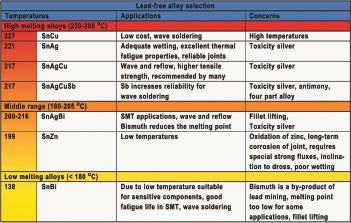
The availability of elements like indium and gold is limited. Therefore, solder costs are high ( > $150 per kg). Price and availability issues reduce the field of candidate elements to Sn, Ag, Zn, Sb, Cu, Bi and Cd. Cadmium is highly toxic and consequently is also banned from the list. Antimony is also a toxic, but only at temperatures above 630°C (the melting point), when toxic fumes are emitted. Bismuth has recycling and fillet lifting issues. Tin is most suitable, exhibiting low cost and excellent physical, electrical and thermal properties. Other elements need to be added in order to drop the melting point to an acceptable level.
Wetting balance tests are indicative of the solderability of alloys. However, wettability in wave soldering is a function of solder temperature, contact time, flux, use of nitrogen and wave configuration. Melting point is also one criterion for alloy selection, since the process temperatures, peak and the time above liquidus for reflow and solderpot temperature, and contact time for wave soldering will very much depend on melting temperature. The lower the melting point, the wider the process window, which makes it easier to design a capable process.
Thermal properties of the alloy are critical. For example, requirements for automotive applications range from –40 to +150°C, where some consumer requirements only have to deal with ambient temperatures of minimum 0 and maximum 60°C. This allows some consumer electronic suppliers to use small amounts of bismuth in order to reduce melting temperatures. All these issues reduce the list of suitable alloys.
Two alloys are suitable for both reflow and wave soldering: SnAg3.5 and SnAgCu (Ag >3.5%). For SnAgCu there are a number of patents and different compositions. For consumer electronics, SnAgBi is a good alternative. SnCu0.7 can be used in wave soldering if cost is a main player and the material must be compatible with higher temperatures, since the solder temperature will need to be at or above 270°C in order to achieve sufficient through-hole penetration.
Flux selection
Since the wetting characteristic of lead-free alloys is not as good as SnPb at lower temperatures, a good flux is very important. Temperatures in lead-free processing have increased, whereas the fluxes that are used for lead-free soldering are the same as used for tin/lead. Flux’s main job (flux/vehicle in solder paste also) is to remove and prevent oxidation. For both wave and reflow processes, activation temperature and time during heating and soldering need to be reformulated for use with lead-free alloys. For the reflow process, this means that the flux should be able to withstand the higher peak temperatures (up to 250°C) at the same time above liquidus. For wave soldering, the flux must be capable of withstanding 130°C preheat and 280°C solder liquidus temperatures for approximately 3s contact time.
VOC-free water based fluxes are the primary candidate, but solder balls and voids must be reduced. New technologies such as dissolving rosin in VOC-free water based fluxes are being investigated right now. Requirements that the selected flux must meet include the following:
• Must comply with legislation and be environmentally friendly
• Must enhance solderability, and be compatible with all materials in the lead-free process
• Must have an acceptable cost
• A VOC-free, water-based flux is recommended. It is expected that the minor objections related to these materials will be resolved soon
Board material and finish
For lead-free soldering processes, we focus on FR4 halogen-free material. Halogen-free boards are desirable because the current EU draft proposes to phase out halogenated flame-retardants by 2004. Again, the materials must be able to withstand the obligatory higher temperatures. This also means that they must exhibit no warpage or delamination of the layers at these higher temperatures. In order to meet these requirements, board materials should have higher Tg numbers of 150°C and higher. Halogen-free material is available for about 30% plus of the price of conventional FR-4.
The majority of PCBs in today’s soldering processes have an SnPb coating on the pads, as well as in the through-holes. This coating is applied using HASL (hot air solder leveling). Organic solderability protectants (OSP) are an alternative finish, which is available for a price in the same range as HASL. OSP is easy processed, and is relatively free of ionic contamination. There are some concerns, particularly low storage life, and excess handling can create problems in process reliability. Multiple soldering processes and soldering at higher temperatures can create problems with regard to oxidation. An inert soldering atmosphere may help.
Electroless NiAu is a second alternative of promise. NiAu is superior to other finishes with regard to shelf life. It is also quite resistant to damage and free of ionic contaminants. NiAu is preferred for higher tempera-tures and multi-soldering processes. The costs are approximately 25% higher then OSP.
Electroplated pure tin exhibits excellent solderability and corrosion resistance. However, this tin is prone to whisker growth. Heat fusing or reflow is used to eliminate whiskers that are promoted by internal stress. Important factors include grain structure and organic impurities in the deposits. Electroplating tin chemistry is robust and well-designed. Tin whisker growth seems to be under control with current technologies.
Component material and finishes
A number of components are already available with lead-free finishes. Alternatives are pure tin or SnCu. In general, the changeover to lead-free finishes for components is expected to be the last part of the conversion, and is certainly the most difficult step of implementation. Component manufacturers have concerns about going lead-free with respect to reliability, as well as higher process temperatures.
Current technology for certain components, such as BGAs and relays, is not so advanced that all of these components can meet the requirements for heat resistance of 260°C for 10s. Encapsulated components with solutions to popcorning and delamination need to be designed and qualified. Compounds used for these components should also be halogen-free. Higher temperatures can cause warpage with connectors and BGAs. Most companies complain that lead-free components are currently not available on the market, as component manufacturers appear to want to produce lead-free products for higher volume demand.
Once all selections for the lead-free materials have been made, it is necessary to review the selected items and compare them with legislation in the countries in which they are intended to be used. Are all materials compatible with the higher soldering temperatures, and do they meet customer specifications? If all materials are within specification and the price is acceptable, then it is time to review machine configuration.
Wave solderingmachine configuration
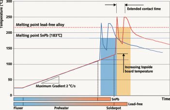
The main difference between SnPb and the lead-free soldering process is the increased melting point of the lead-free alloy. This requires higher preheat temperatures; the thermal shock at the entry of the first wave must not exceed 100ºC.
VOC-free, water-based fluxes are recommended for lead-free soldering because they can meet the higher temperature requirements, and are environmentally friendly. Due to the different thermal properties and the viscosity of water and flux, suppliers do not support foam application of water-based fluxes, so the machine must be retrofitted with a sprayer in the event that a water-based flux is used. If it is not, a more robust, heat-resistant flux must be selected for foam fluxing; the foam tube and density control unit have to be verified for this flux.
Spray fluxing a VOC-free, water based flux requires some special attention. First, the atomizing air should be increased (with approximate 0.2bar) in order to achieve the finest possible droplets. A special small fluid cap might be required to spray an amount of flux, which is almost 1/3 of the amount of a no-clean alcohol based flux. The spray pattern can be inspected with a glass plate or water-sensitive paper. The through-hole penetration of the flux can be examined with the fluxometer of ECD.
The topside temperature of the board will increase to 110 to 130°C at the end of the last zone (to limit the thermal shock at the entrance of the first wave). The best way is to heat-up the board as quickly as possible to 100ºC. Then, continue with hot air(forced convection) for optimal evaporation of water (in through-holes, underneath components, between pallets and boards). Depending on the type of production, the third preheat zone can be hot air, infrared (special for mixed production) or calrod heaters. It is essential for the VOC-free fluxes that all water should be evaporated before entering the first wave to prevent spattering. Proper preheating requires at least a heating length of 1800mm for conveyor speeds of 120cm/min and higher. Particularly for high-speed soldering ( >180cm/min), a preheating length of 2400mm is recommended. If high throughput is a hot issue and decreasing conveyor speed is not allowed, a longer preheating unit may be required, also higher solder temperatures.
Solderpot temperatures will increase. The temperature will depend on the alloy. For AgSnCu (melting point 217ºC), the solder temperature will be from 250 to 270ºC. For high melting alloys like SnCu, the temperature will be 260 to 280ºC. In general, the higher the solder temperature, the better the solderability, and the shorter the contact times. The contact time is defined by the conveyor speed and the wave former configuration and settings. Solderability can be improved by using nitrogen, a stronger flux or a ‘smart’ wave.
Reflow solderingmachine configuration
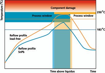
For reflow soldering, the implementation of lead-free alloys impacts temperatures, and consequently heating profile. Increasing the melting temperature means that the process window is becoming narrower, due to the fact that both time above liquidus and the maximum allowed temperature of 250°C (to prevent component damage and board delamination) do not change.
Board warpage will become an issue if temperatures rise, and therefore are more critical for the materials in the process. A proper board support or gripper system might prevent board warpage. Heat transfer becomes more important as the process window shrinks. There are three principles of heat transfer that can be applied in a reflow process. A choice should be made between radiation, hot air/nitrogen convection or vapor phase. Lamps (radiative) will not meet lead-free requirements, and throughput in a vapor phase process is too low. This leaves hot air convection as the most suitable way.
Using nitrogen is recommended for OSP finishes. An inert atmosphere will prevent oxidation and improve wetting; however, use of an inert gas blanket also adds cost to the process, and may introduce other possible defects such as tombstoning. Process specifications such as oven configuration, heating and cooling length will be defined by a number of factors such as required machine throughput, board dimensions, distance between boards, required exit temperature and temperature profile based on the solder paste and component specifications.
Heating zone setpoints are determined by the soldering profile of the product. Several peak zones may be required. Try to achieve the smallest temperature differences at the entry of the peak zone as possible. The goal is to stay long enough above liquidus temperature for the coolest spot on the board to solder properly, and not exceed the maximum limitations for the hottest spot on the board.
The melting point of the alloy plays a dominated rule in this process. Therefore, it is highly unlikely that alloys with a higher melting point, such as SnCu (227°C), will be used for reflow. Alloys like SnAgBi (melting range 200 to 216°C), SnAgCu (217°C) and SnAg (221°C) are recommended.
Long-term reliability of an SMT solder joint is affected by the cooling rate of the paste during solidification. In the lead-free process, even more attention should be paid to cooling aspects since we have to deal with a complexity of components and substrates. Cooling has a direct and profound effect on the following:
• Time above liquidus
• Solder joint grain structure
• Protection of OSP coatings
• Product exit temperature
• Material damage
• Residual stresses in solder
It is desirable to select reflow equipment that will offer multiple options and flexibility in terms of controlled cooling, which is essential in lead-free soldering where temperature control is more critical than ever. It can be argued that in general, there is a lack of standardization in lead-free soldering, and this is true with regard to cooling.www.vitronics-soltec.com
EPP 152
References
Y.Zhang, G.Breck, F.Humiec, K.Murski and J.A. Abys: An Alternative Surface Finish For Tin/Lead Solders – Pure Tin. Lucent Technologies Bell Laboratories, Murray Hill, NJ
W.James Hall: Cooling Parameters in Reflow Soldering. Vitronics Soltec, Stratham, NH
Useful lead-free web addresses
Zusammenfassung
Zwar hat die EU ihre Direktive zur endgültigen Einführung der bleifreien Elektronikmontage in einem Akt blinder Hörigkeit gegenüber kurzsichtigen Einflüsterungen von 2004 auf 2008 verschoben, doch kommt der Druck für einen schnellen Übergang klarerweise ausSüdostasien. Europäische Provinz-Lobbyisten sind hier nicht gefragt. Will man in der europäischen Elektronikmontage nicht – ähnlich wie in der Halbleiterfertigung – auf hintere Plätze verwiesen werden, muß man jetzt handeln. Damit von den bisher eher akademischen Erörterungen des Themas eine direkte Übertragung zu den praktischen Fragen direkt in Fertigungslinien erfolgt, werden wir in einer Reihe von exklusiven Beiträgen hier für weitere Klarheit sorgen.
Résumé
L’UE a repoussé de 2004 à 2008 sa directive relative à l’introduction définitive du montage électronique sans plomb dans un acte de sujétion aveugle à des considérations à court terme, mais la pression pour un changement rapide vient clairement d’Asie du Sud-Est. Les lobbies provinciaux européens ne sont ici pas à leur place. Si l’on veut éviter que l’assemblage électronique européen soit relégué aux dernières places comme c’est le cas de la fabrication de semi-conducteurs, il est impératif d’agir maintenant. Afin que les débats plutôt académiques laissent la place aux questions concrètes et à des répercussions pratiques sur les chaînes de fabrication, une série d’articles exclusifs sera publiée en vue d’assurer plus de clarté en la matière.
Sommario
È vero che la CE ha rimandato dal 2004 al 2008 la sua direttiva per l’uso di impianti di montaggio di componenti elettronici senza uso di piombo, seguendo dubbiosi suggerimenti, ma è chiaro che la necessità di un passaggio il più rapido possibile ha le sue origini nel sud-est asiatico. Il lobbismo di alcune province europee arreca più danno che vantaggio. Se nel settore europeo dei montaggi di componenti elettronici, come già successo nella produzione di semiconduttori, non si desidera retrocedere rispetto alla concorrenza, è necessario agire ora. Per fare in modo di poter passare da discussioni accademiche all’applicazione pratica delle tematiche nelle linee di produzione provvederemo a chiarire tale argomento in una serie di esclusivi articoli.
Unsere Webinar-Empfehlung
10.10.22 | 10:00 Uhr | Conformal Coating ist ein wichtiges Verfahren, um elektronische Baugruppen vor dem vorzeitigen Ausfall zu schützen. Damit bekommt der Beschichtungsprozess eine immer höhere Bedeutung. Dabei ist die Auftragsstärke ein wichtiges Qualitätskriterium. Nur eine…
Teilen:


