Laser structuring developed by Siemens PL is a next-generation technology that uses a CAD data-controlled laser to create microstructures onto PCBs for advanced component, such as BGA, CSP or flip chip.
To follow miniaturization, correspondingly finer PCB conductors are required, calling for structures of50em and smaller. Laser structuring meets the challenge in producing microstructures economically and efficiently.
Routing of two conductorsbetween adjoining balls inan area-array package with 0.8mm pitch and 0.5mm ball diameter requires lines and spaces smaller than 75em. There is, however, more to high density printed (HDI) PCBs than fine or ultra-fine structures: through-hole diameters have to be just as small, and finer lands around the holes, as well as smaller pads are necessary. This is where laser structuring comes into its own. On the copper and tin coated PCB, a CAD data-controlled laser creates conductors by outlining the circuitry so, the insulation between the conductors is created by ablating the metal. Further steps include etching the copper and removing the tin. Co-operation with Cimatec, a specialist for immersion tin, has perfectly matched the process.
If a laser is used only to generate insulation between the conductors, and the remaining copper surface is left (max copper design), the PCB processing time can be cut drastically. A high-speed laser achieves removal rates of up to 1.500mm / sec. The positional accuracy is within 10mm with 4-sigma. Laser structuring enables the pad diameter on the PCB to be reduced from 300 to less than 100em, and the component pad pitch from 0.8 to 0.5 or 0.3em. This technology creates 50mm structures with more than 80% yield. Laser structuring reduces the number of steps in the process. Expenses for cleanroom, film, mask, and photoresist, as well as the disposal cost for environmentally harmful materials and residues are also significantly minimized. Using the laser also allows different layouts to be created more flexible; only the CAD data have to be modified. Although finer structures are still not required for many mass applications, some multi-pin ICs already require those high-density PCBs. One solution is partial high density, or processing only selected areas, which has the advantage of doing away with the expensive technology. This approach saves space for routing high-density versions. Combining laser structuring with the conventional PCB production requires process-ing of only fine-structured areas; the rest is processed using conventional technology. gbw
Fax +49-911-895-5217
EPP 165
Unsere Webinar-Empfehlung
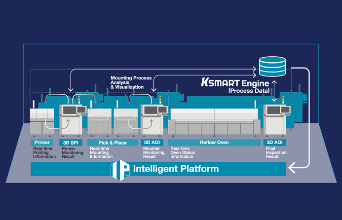
Die Nutzung der 3D-Mess- und Prozessdaten bringt die Produktionssteuerung auf die nächste Stufe. Echte 3D-Messung ermöglicht KI-basierte Prozessmodellierung zur Vorhersage von Parameteränderungen und -defekten oder zur Ursachenanalyse bis hin zu einzelnen Werkzeugen und Best…
Teilen:


