The stacked chip-scale package (S-CSP) is one of the most important advances in laminate technology, and is the industry’s first low-cost, high volume three-dimensional device assembly method. Its development and application has been driven widely by all kinds of portable electronic products, and, even more, it’s an enabling technology for the ongoing miniaturization and higher density of functions and features in mobile gear.
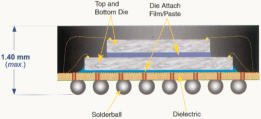
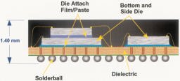
The biggest benefit of stacked CSPs is the fact that such a component, comprised for example of two single dies and a passive, takes the same footprint as a conventional IC. The laminate serves as the substrate, providing the basis for very thin advanced packages. The substrate is a film-like dielectric with a core thickness of 100 or 150mm, featuring up to four layers for interconnects. Amkor’s technique is able to combine up to three of these dies which form an encapsulated component only 1.4mm thick, including the solder balls for the board connect which have a diameter of .3, .4 or .46mm. This produces a low-profile package, a sys-tem-in-a-package (SiP) with a standard outline according to JEDEC MO-219. SiP devices are easier to realize than classical SoC (system-in-a-chip), because for every single die the optimal frontend process can be employed (yield, time-to-market), and such a SiP is also the optimum solution for customized device scalability.
Amkor, founded in 1968, covers a wealth of semiconductor packaging expertise, and provides every necessary step in this process as one-stop-shop on a global scale. Its enormous portfolio leads from packaging design and characterization, to wafer foundry, to test, and the advanced packaging as the core technology. The risk and investment for a customer, implementing new packaging methods, is therefore small and easy to calculate. At the same time, full access to leading-edge technology is available. Amkor is the unsurpassed market leader in substrate technology, covering about 50% of the world market for the laminate-based BGA technology. In total, the company’s 3D packaging strategy is comprised of many technologies such as stacked CSP (IC or ASIC plus memories), stacked die leadframe (TSOP, QFP, MLF), flip stack (with flip-chip and wire bond), die stack on PBGA, fleXBGA and die/ package stack. Component-internal interconnects are provided by wire bonding technique; passives can also be easily integrated into SiPs.
With the S-CSP technique, the company leverages its existing manufacturing capabilities for BGAs and proven packaging expertise, while adding the possibility of mounting one die on top of another. These packages, available in many different configurations, combine thin-core substrate material, wafer backgrinding experience (down to a die thickness of only 175mm), and the BGA technique offers doublethe memory capacity for increased de-vice functionality, while allowing sizereductions. It also has the flexibility to merge customized memory designs with off-the-shelf parts to further reduce system costs.
Stacking – road to higher density and functionality
What are the forces behind this advance? For the development of semiconductors, it is generally recognized that Moore’s Law holds true – the number of transistors or functionality has doubled every 18 months in contemporary history. As an inevitable result, the rate of integration has finally outpaced the wiring/space capacity of PCBs, where features are measured in the submillimeter range, compared to the much finer submicrons achieved in ICs. This means that the second (package) level interconnection density is limiting the ability to deliver the functionality represented by systems-on-a-chip (SoC) concepts.
This has created a tough challenge because, while the market is demanding size, weight and cost reductions for portable products, it is nevertheless expecting functionality increases. One way to provide the performance necessary, without outpacing the ability of the PCB to wire higher levels of silicon integration, is through 3D package arrays that deliver volumetric density through vertical stacking. This method integrates multiple chips in a package to provide higher levels of functionality than can be achieved through multiple package solutions technologies.
Plenty of pros for S-CSP
S-CSPs, integrating higher density devices, along with their higher I/O counts, may utilize die-to-die bonding and high density interconnect (HDI) substrates to handle higher wiring densities at package level. As a result, these devices enable both a reduction in the PCB wiring den-sity together with a significant reduction of the PCB area required. This reduction can result in significant board cost cutback.
The direct savings achieved at final assembly, through integrating multiple devices onto one package, combine with indirect savings associated with fewer components to test, procure and rework. This leads to minimized cost of ownership for 3D packaging that utilizes chip sets, high levels of silicon integration or large memory blocks. As an early adopter of chip-scale packages, the mobile phone manufacturers have enabled CSPs to evolve rapidly and become more cost-effective in serving a wider range of applications. Industry forecasters agree that the CSP currently has the highest growth rate among all package types, due to the wide range of applications and devices driving its adoption. Prismark prognoses that 3D packaging could see up to a 10% share of all IC packages by the year 2002. The forecast says that this could be as many as 40bn components based on stacking technologies. According to the researchers, this will represent the fourth wave in packaging innovation.
Increasing functionality
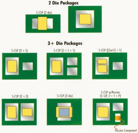
3D packaging allows for increased functionality, including greater memory capacities, thus enabling endproduct size reduction, which is key for all mobile gear. As more features and functions are integrated along with an increase in bandwidth and memory capacity, S-CSP adoption will continue to expand beyond just the stacking of flash and SRAM devices. Incursions will continue into the stacking of ASIC, mixed-signal and processor devices, including those with DRAM and other high-density memory devices. The die sizes and bond patterns can require a unique range of die stack and side-by-side configurations to optimize the placement of multiple devices within a SiP.
Some emerging applications are even evaluating the stacking of RF devices on top of logic, with flip-chip bumps for cost-effective integration of higher frequency devices including global positioning systems (GPS), radio modules and Bluetooth components. For advanced mobile phones, three-chip integration in S-CSPs has been developed to combine baseband and memory functions in smaller, more cost-effective packages. Advances in wafer thinning, die stacking, die-to-die wirebonding and HDI substrates enable S-CSP to be optimized for the specific requirements of the application or devices to be integrated. Amkor as the market leader has the experience and expertise to customize these configurations to deliver high performance, and yet still meet cost targets.
Design de-partitioning for cost/performance benefits
High level functionality currently could only be found on a SoC, but the S-CSP technology enables semiconductor suppliers to look at design de-partitioning for cost/performance optimization. A chip design can be partitioned into multiple devices based on different processes best suited to analogue, digital and memory functions- as opposed to complex mixed-signal or mixed-technology SoCs. The result is a SiP (system-in-a-package), to realize faster, easier and with higher yield. Many fabless semiconductor suppliers are positioning design de-partitioning and 3D packaging technologies as part of their product roadmaps and system integration plans. An emerging trend is to use triple chip stacking to meet the higher storage and faster time-to-market requirements, while developing high-density memory chips. Amkor has focused its efforts on the development and qualification of a range of advanced 3D packages to handle various device combinations and emergent end-product applications. Memory stacking is still the dominant application.
Considerations for high volume applications
The many benefits of S-CSP are proven by the rapid adoption into portable products and the high uptake expected by emerging or converging applications. However, some important considerations must be anticipated before successfully deploying 3D packaging technologies into ultra-high volume applications:
Because S-CSPs are essentially space efficient MCMs, fully tested, known good die (KGD) and burn-in capabilities at the wafer level are required to achieve high yields at the package level. Since full functionality testing is often a challenge with multi-chip packages, it is critical that the quality of the die going into the package be well understood, and that the substrate and assembly yields be near 100% in order to meet cost and quality requirements. It is critical that die shrinks be projected or carefully managed to avoid package changes which may require re-qualification and lead to excess inventory and costs.
Sourcing from multiple foundries can be a challenge because relative die sizes can vary substantially. To optimize cost and performance for system-in-a-package (SiP) and multi-chip-package integration (including stacking), a close collaboration between an OEM, IDM (integrated device manufacturer) and a full service microelectronics manufacturer can provide tremendous advantages.
In an ideal situation, the different IC designs should be optimized for stacking both in terms of die size, stack-up and die-to-die bonding. The drive to achieve 1.4mm maximum package height for three die stacks and 1.2mm maximum for two die stacks has put tremendous pressure on backend, wafer and die-handling during the assembly process to ensure high yields.
The location of wirebonds in three dimensions along the length and loop heights of the wire connections must be considered to avoid shorting or cross talk between tiers. The diameter and maximum length of the wirebond connections must be con-sidered with respect to the extent ofwire sweep and to ensure high assembly yields.
Collaboration between Amkor and Zuken has resulted in an effective design tool that will help optimize design for ultra-high manufacturability. This 3D tool can address an unlimited range of die size, location/rotation, stack-up and bond pad placement options to facilitate S-CSP designs. In addition, 3D wire-profile and clearance design rule checking is being developed to ensure that the stack-up will be capable of manufacturing at high volumes, yields and throughputs.
EPP 188
Zusammenfassung
Aufeinander gepackte ungehäuste Chips (Dies), sind eine Lösung, um auf kostengünstige Weise die Funktionsdichte insbesondere von tragbaren bzw. kompakten Geräten weiter zu erhöhen. Diese Stacking oder 3D-Packaging genannte Methode (Stacked Chip-Scale Package, S-CSP) ermöglicht derzeit, bis zu drei Dies aufeinanderzupacken und dennoch eine sehr minimale Höhe im Bereich um 1,5mm einzuhalten.
Résumé
Les puces sans boîtier empilées (Dies) sont une solution pour accroître de manière économique la densité fonctionnelle des appareils portables et compacts en particulier. Cette méthode appelée Stacking ou 3D-Packaging (Stacked Chip-Scale Package, S-CSP) permet d’empiler actuellement trois Dies sans dépasser une hauteur minime de 1,5mm.
Sommario
I Dies, vale a dire chip nudi pacchettati l’uno sull’altro, rappresentano una soluzione finalizzata ad aumentare ulteriormente in maniera economica la densità funzionale soprattutto di apparecchi compatti e portatili. Questo metodo, chiamato Stacking o 3D-Packaging (Stacked Chip-Scale Package, S-CSP) permette tutt’ora di pacchettizzare l’uno sull’altro sino a tre Dies mantenendo comunque un’altezza molto bassa di ca. 1,5 mm.
References
M. Kada, L. Smith, ”Advancements in Stacked Chip Scale Packaging (S-CSP) Provides System in a Package Functionality for Wireless and Handheld Applications,“ 2000 proceedings Pan Pacific Microelectronics Symposium.
T. Swirbel, ”Chip Scale Package and Multichip Module Impact on Substrate Requirements for Portable Wireless Products“, International Journal of Microcircuits and Electronic Packaging, Volume 23, Number 3, 2000
Prismark Partners, B. Swiggett, Amkor Technology’s 3rd Annual Customer Symposium, November 1999, Santa Clara
TechSearch International, ”BGA/CSP Development Update Service Q3 2000“
Unsere Webinar-Empfehlung
.png)
Auch dieses Jahr präsentiert Koh Young wieder aktuelle Trends und „State of the Art“ Technologie aus der optischen Inspektion und 3D-Messung auf der Productronica in München. Aber wir alle kennen das Problem voller Terminkalender, Reisebeschränkungen oder fehlender Zeit, um in…
Teilen:


