Assembly and packaging is the bridge between the silicon and the board, creating the functionality of electronic systems. Therefore, packaging design can no longer be made independently of chip, board, assembly process, environmental aspects and the whole system. Wafer-level packaging (WLP) became one of the most challenging backend issues.
Michael Töpper and Herbert Reichl, Fraunhofer IZM, Berlin; Dietrich Toennies and Elmar Cullmann, Karl Suss
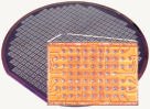
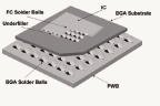
In this technology, the die and the package are manufactured and tested on the wafer, before singulation. If there is no packaging after dicing, we define this technology as a true WLP concept. The package is completed directly on the wafer, then singulated into many dies for assembly in flip-chip fashion. A WL package features a real chip size rather than chip-scale format due to the processing. The unique feature of the wafer-level approach for CSPs is that there is no bonding technique inside the package. A redistribution process to enlarge the pad pitch of the ICs is common for all wafer-level CSPs.
There is confusion in the industry over the nomenclature of the existing and proposed wafer-level packaging concepts. The key point is whether the devices are further packaged before assembly. For high I/O components such as microprocessors and ASIC, the chips are mounted on carriers before SMT attachment. Therefore, these are not true wafer-level packages. However, their bumping is usually performed in a wafer-level technology. The acronym FCIP (flip-chip-in-package) should be used for this approach.
Market trends: what NEMI says
Packaging roadmaps depend heavily on applications. The U.S. National Electronic Manufacturing Initiative (NEMI) has categorized these into the following product sectors:
- a) Low cost: up to $300 (consumer appliances, microcontrollers, disk drives, displays, etc.)
- b) Hand-held: up to $1000 (battery-powered mobile products, mobile cellular phones, etc.)
- c) Cost performance: up to $3000 (notebooks, desktop PCs, etc.)
- d) High-performance: more than $3000 (high-end workstations, servers, avionics, etc.)
- e) Harsh (under-the-hood and other hostile environments)
- f) Memory (DRAM, SRAMs)
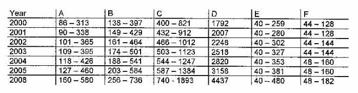
The I/O count is a very important criterion for the selection of the most cost-effective and reliable packaging technology. For the year 2005, the technology roadmap for semiconductors is proposing 120 to 600 I/Os for low-cost and hand-held applications, and up to 1400 or 3200 respectively for cost-performance and high-performance applications, coupled with on-chip RF performance of up to 2GHz. The number of bumps for FC technology will increase due to the electromigration limits of the solder interconnects. Though the mean-time-to failure of a bump is a function of the passivation opening and the current flowing through, a higher pitch will require more bumps in parallel for power and ground. The roadmap for example predicts for the cost-performance microprocessor to draw an average current of 80A (96W at 1.2V). With a bump pitch of 150µm and a passivation opening of 65µm, the current limit is 95mA per bump at 80°C and 45mA at 100°C chip temperature. The current (voltage and ground) will require 840 bumps each for a total of 1680 bumps for the supply if the operating temperature of the chip is 80°C, and 3550 bumps at a temperature of 100°C. The table shows trends for the increase in pincount in different applications over the years.
This increasing density of I/Os on the chips has already driven the pitch of peripheral pads down to 70µm which is within the capability of wire bonding tools. The issue of wire bonding is its sequential and therefore time-consuming process. Not the feasibility is the problem, but the speed to provide all interconnections. Bumping is done on wafer level; this means that all chips of a wafer are bumped in the same single process step in one stroke. Wafer-level process steps are independent of the number of dies and the corresponding number of bondpads on the wafer. Increasing the wafer diameter leads to more dies within the same process in contrast to other types of flip-chip-in-package, where each die has to be individually mounted to a carrier or interposer. So, WLPs have the advantage that the cost per single chip package will decrease by increasing the wafer size or by decreasing the die size.
Take for example a simple cost calculation with a peripheral bond pad density of two pins per square mm (200 pins for a 10mm x 10mm chip). The cost limit for an established SCP process is around 1 cent per I/O. This gives approximately $300 per 150mm wafer and $550 per 200mm, assuming nearly 100% production yield for frontend processing and redistribution. This is much higher than the cost for thinfilm redistribution and bumping in volume. Therefore, packaging costs for the inevitable bad dies are not a significant argument. Testing of the dies can be done after redistribution and bumping. The result is known-good-packages (KGP) instead of known-good-dies (KGD), saving further expenses.
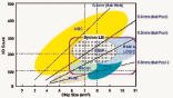
As WLP is an on-chip technology, it is restricted to the number of I/Os per die for a given area-array ball pitch. All ball pitches for WL-CSP are above 0.4mm, this means that the main application of WL-CSP is low and medium pincount devices.
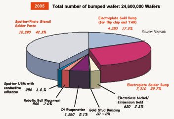
The strongest demand for WL-CSP is driven by memory, automotive and low-cost consumer applications. Basic technology for WLP are the photolithography to pattern the high-density runners, and a combination of sputtering and electroplating to guarantee adhesion between the layers and a low resistivity of the metallization layer. For all other high I/O pincount devices, the trend is leading to bumping technologies which guarantee high yield at low cost. Marketanalyst Prismark expects anotable increase for solder bumping using electroplating.
The reason for this is the capability of electroplating in combination with photolithography to bump chips with peripheral or area-ar-ray pad pitches down to 50µm. This high-yield technology also leads the wayto the potent gold bumping application market, focused on spaces between pads of 10µm or less. No other technology is able to fulfill this demand.
The 300mm transition
For further cost reduction in the frontend, processing technology is moving now from 200 to 300mm wafers. Such technologies are usually developed for high-volume devices such as DRAMs. Processing of SRAMs, microprocessors and ASICs will follow this trend with a short delay. It is expected that the demand for 300mm wafers will increase to more than 17% in the year 2005.
In 2001 a total of six, and in 2002 a total of fourteen 300mm waferfabs are scheduled to start production. The transition to 300mm technology is focused mainly on frontend equipment and certain automation issues. Together with the growing need for wafer bumping and wafer-level packaging, backend processes also need to be performed at the wafer level. For the wafer-level packaging technology, these steps consist largely of sputtering the UBM (under bump metallization) and the seed layers, deposition and photolithography of thick resists, electroplating Cu, Ni, Au and solder, etching the metals and eventually dicing.
The question comes up then, whether there are WLP technology limits in the transition to 300mm. Electroplated solder bumps or the rewiring metallization are made by passing current through a thin metal layer on the wafer that acts as the seed layer for electrodeposition. The requirements for the seed layer are very high homogeny and adhesion to the die metallization or passivation respectively to secure high reliability. All metal oxides of the wafer metallization have to be removed prior to the metal deposition to guarantee good electrical contact. This is done by back sputtering or ICP etch in the sputtering tool, just before the metal is deposited. To prevent interdiffusion of the on-wafer level into the die-metallization, a barrier is deposited underneath the seed layer. The reliability of a bump relies on its under bump metallization (UBM). All layers can be deposited with high yield and excellent uniformity on 300mm wafers using sputtering technology.
Cluster tools have enough flexibility for different metal stacks and assure low cost by short process times. The shape of the metal structures are determined by the resist mold which has to be uniform over the entire wafer surface. A sufficient depth-of-field of the tool is necessary to structure resist layers of up to 100µm and above. The photoresist should have a clear edge bead removal zone (EBR) around the outer side of the wafer. This zone should be designed out of any active devices on the wafer. This can easily be realized using a full-field mask aligner. All dies and all necessary auxiliary structures can be exposed in one shot. Such auxiliary structures could be dummy bumps at the wafer edge that guarantees a more uniform current density through the plating mask and, therefore, a uniform bump height over the entire wafer will be attained. To structure a resist-free ring at the edge of the wafer is much easier using full-field mask aligner. This ring contact of the platter makes the electrical contact to the blank seed layer of the EBR zone. This ensures optimal plating current uniformity. Edge plating, which negatively impacts the bump height distribution over the wafer, is prevented by an elastomeric seal ring over the photoresist edge. At this stage, close co-operation between sputtering, photolithography and the electroplating process is an essential factor to guaranteeing success for a high-yield process.
A group of semiconductor equipment suppliers have joined forces with the Fraunhofer Institute for Reliability and Microintegration IZM in order to form a group aimed at optimizing equipment for wafer bumping and wafer-level packaging technologies. The SECAP (Semiconductor Equipment Consortium for Advanced Packaging) addresses semiconductor packaging. Initial participants include Karl Suss (Germany), Semitool (USA) and Unaxis (formerly Balzers from Lichtenstein), equipment suppliers in photolithography, electroplating and sputtering, and joined by Image Technology from the US, a manufacturer of large-area photomasks (now member of the Suss group). The Fraunhofer IZM/Berlin has been acting as technology consultantand center for process sequence integration (see EPP Europe #1/2-2001).
The consortium offers reliable partnerships to customers. First initiative was the start of a bumping project, in order to develop and validate 300mm wafer process equipment for the conversion to high-density interconnect technologies. For a cost-efficient production of systems-in-a-package, strategy has to be developed in close conjunction to the development in the frontend.
The main challenge of 300mm technology on the equipment side is seen in the availability of precision 14-in photomasks, for full-field exposure of 300mm wafers with sufficient intensity uniformity and control within the same specs as for 200mm, achieving uniform UBM layers by sputtering and uniform plating heights. SECAP demonstrated that there are no barriers for the move to 300mm. First bumped wafers based on an electroplating process were presented; therefore, WLP is ready for 300mm.
EPP 192
Zusammenfassung
Mit zunehmender Funktionsdichte in elektronischen Geräten ist natürlich auch die Packungsdichte der Schaltung eine kritische Aufgabe geworden. Hat man sich bisher bei Advanced-Packages (CSP, BGA Flip-Chip) noch auf traditionellen Ablauf mit Packaging nach der Chip-Vereinzelung gestützt, so setzt die weitere Miniaturisierung beim ungetrennten Wafer (Wafer-Level Packaging) auf.
Résumé
Compte tenu de la densité fonctionnelle croissante des appareils électroniques, la densité d’équipement des circuits est aujourd’hui critique. Alors qu’on tablait, jusqu’à présent avec les Advanced-Packages (CSP, BGA Flip-Chip), sur le déroulement traditionnel avec le Packaging après la séparation des puces, la miniaturisation croissante intervient avec le wafer non séparé (Wafer-Level Packaging).
Sommario
Con l’aumentare della densità funzionale degli apparecchi elettronici, anche la densità di pacchettizzazione dei circuiti elettronici si é trasformata in un compito critico. Se nel caso degli Advanced-Packages (CSP, BGA Flip-Chip) si é fatto sino ad oggi ricorso alla tradizionale sequenza, che prevede il Packaging dopo la singolarizzazione dei Chip, la sempre maggiore miniaturizzazione punta sui wafer ancora interi (Wafer-Level Packaging).
Unsere Webinar-Empfehlung
.png)
Auch dieses Jahr präsentiert Koh Young wieder aktuelle Trends und „State of the Art“ Technologie aus der optischen Inspektion und 3D-Messung auf der Productronica in München. Aber wir alle kennen das Problem voller Terminkalender, Reisebeschränkungen oder fehlender Zeit, um in…
Teilen:


