The demand to eliminate the use of lead (Pb) in the electronics industry is constantly growing. Here, we want to put some extra information into the ongoing discussion on lead-free assembly, especially in regard to solder paste, board material and the reflow process.
Klaus Brodt, SMT/Germany,Simone Peters, Josef Schneider, Loctite/Germany, Volker Clausen, Straschu/Germany
The board material
The lead-free process affects PCBs in two ways: first, the surface of the pads has to be lead-free, and second, the base material has to be compatible to higher temperatures that will be needed for the soldering process. Eventually, the suitability in manufacturing will be decisive for the method preferred. At least for a period, different finishes will be used. There are several alternatives available for lead-free surfaces:
•Tin (Sn)
•Nickel-Gold (Ni-Au)
•Silver (Ag)
•Palladium (Pd)
•Universal finish
•Organic coating
•Alternative materialsfor hot air leveling (HAL)
Lead-free solder requires higher process temperatures. This results in a higher stress level for PCBs. A solution can be base material with a higher softening point (vitreous point Tg). One possibility is to employ FR4 with a Tg of 150°C. Such material can be used without problems, and can replace the current substrate (Tg 135°C) at almost no additional cost. Stra-schu has already decided for this material. Another option is to introduce a Tg system of 180°C. These materials have to be qualified again. Availability and price will have to be settled after there is more demand from the market.
The problem will be even more complicated for PCB manufacturers by another condition that will become effective in the year 2006 as part of the EU’s WEEE legislation. Additionally to lead, some compounds will also be banned. This applies to brominated flame-retardants such as TBBA (tetra bromobishenol A), used in FR4 material. Alternatives are available, however. At least for the moment they are rarely used in Europe. A significant disadvantage is that until now they are only available with a Tg of 135°C. Materials without FR4 (cyanide ester, BT laminates and polyimides) do not have the problem with flame-retardants. Until a final solution to this problem is found, Straschu will continue its way (FR4 with Tg 150°C).
The solder paste
The U.S. NCMS (National Center for Manufacturing Sciences) has tested more than 75 different alloys and could not find one to replace conventional solder paste at unchanged process conditions. Possible lead-free alloys are based on pure tin with a melting point of 232°C. But pure tin is not suitable as it forms a brittle, granular structure at lower temperatures. The melting point of pure tin can be reduced, combined with different elements. A wide range of metals have been tested for their suitability as alloying elements. Many of them have restrictions such as price, availability and toxicity. Silver, copper, bismuth and indium are generally regarded as best solutions, but the use of bismuth and indium is limited by their availability.
Suitable lead-free solder pastes should show the following attributes:
•Sufficient availability
•Compatible with existing processes
•Acceptable melting points
•Acceptable solidity of the solder joint
•Thermo and electric conductivity comparable to conventional paste
•Rework compatible
•Non toxic
•Reasonable price
In the literature, we found several alloys made from the mentioned elements, which are recognized to be suitable for lead-free assembly. Preferred are binary alloys with copper or silver, and respectivelyternary combinations that include both of them: 99.3Sn0.7Cu with a melting pointof 227°C; 96.5Sn3.5Ag with 221°C; and 95.5Sn3.8Ag0.7Cu with 217°C.
The first two are eutectic alloys; both contain the intermetallic phases Ag3Sn and Cu6Sn5. The AgSn alloy tends to build Cu6Sn5 at copper containing contacts. Adding copper to the SnAg alloy diminishes the tendency for intermetallic growth at contact points, and reduces the melting point of the alloy. Furthermore, the ternary alloys show improved wettability, creep property and resistance concerning thermal variations. Bismuth, antimony or indium may be added to further lower the melting point. However, with a growing number of metals in an alloy, also the number of possible intermetallic phases is increased, and thus it is difficult to predict its behavior.
Also, low temperature alloys have been tested, for example eutectic 42Sn58Bi with a melting point of 139°C. Other combinations that are close to being eutectic, as well as ternary alloys which in addition contain indium, copper, gold, antimony or others are known. Low temperature alloys may for example be used in appliances where the temperature requirements are below 100°C. The problem with alloys containing a high share of bismuth is their availability. If the industry decides for an alloy with a high content of bismuth, all resources would be depleted within 15 to20 years.
Adaption of the flux
During the solder process, high temperature pastes tend to have a large build-up of bubbles. These cavities reduce the reliability of the solder joints. Especially stress caused by thermal variations is a starting point for cracking of solder joints. In most cases, the solvent in the flux causes the bubbles. This effect can be avoided by using solvents with an evaporation point above the reflow temperature of the alloy. For lead-free paste, it was observed that the same flux used for conventional SnPb alloys tends to build bubbles. Replacing it by a substance with a boiling point above 217°C significantly reduces the tendency for building bubbles as well as the dimensions of the cavities.
In developing flux for lead-free solder paste, it is one of the most important factors to select a proper solvent with the aim not only of fulfilling the regular requirements, but also to raise it to a melting point above 220°C. The rosin and activator in traditional flux may also be used in lead-free formulations. This is because the first part of the reflow profile is comparable for both types of pastes. Just the peak temperature has to be adapted.
The lead-free solder paste 3835 of Loctite contains ternary alloy. This alloy forms good solder joints at a comparably low melting point. Therefore, the temperature for soldering can remain low enough to avoid interference with temperature sensitive components or PCBs.
The user of lead-free solder paste is primarily interested in which changes have to be made in the process technology of existing SMT lines in order to guarantee a comparable quality of solder joints. Four different process steps have to be considered for this: stencil printing, soldering, inspection of solder joints and their rework.
Stencil printing and reflow soldering
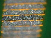
Loctite has performed various printing tests with the lead-free product 3835 (Sn95,5Ag3,8Cu0,7). For this purpose, laser-cut metal stencils with a thickness of 100 to 150µm was used; the surface of the PCB was Ni-Au. The tests have shown that this paste can fulfill the requirements: high printing speed of up to 150mm/s, pause of up to 40-min between printing strokes, and a processing time of 10-hours. Paste deposits for fine-pitch components with an array pitch of 0,40mm can be realized. Therefore, it is ensured that the existing printers, the metal stencils and the metal squeegees can be used for the print of lead-free solder.
The aim of the soldering process is to produce reliably high-quality solder joints at lowest possible temperatures in order to avoid thermal damage of assemblies. The formulation of the paste (metallic powder, flux and other constituents) determines the required temperature profile for the reflow process. The melting point of the SnAgCu alloy is 217°C, compared to 179°C for Sn62Pb36Ag2. To produce a good lead-free solder joint, temperatures of 160 to 170°C in the preheating zone and approximately 235 to 250°C in the peakzone are necessary. The total heating time should be about 3 to 4-min with 40 to 60s above liquidus. Efficient forced-convection ovens can handle these increased requirements, while older IR units and some convection ovens show limitations. In some lines, IR ovens are still being used. However, due to the high temperature differences between heavy and light components, between light metal surfaces and dark plastic and due to the shadow effect, this type of oven has almost disappeared. The disadvantages will be increased in front of higher process temperatures, and those ovens will have to be replaced.
Vapor phase soldering reveals also some disadvantages based on physics. The liquid used for generating the vapor-saturated atmosphere determines the maximum temperature. If the technology ofthe past with minimum soldering tem-peratures (20 to 25K above meltingpoint) is transferred to lead-free assemb-ly, then a liquid should be used with a boiling point of 237 to 246°C. However, if the initial operating temperature does not provide the desired results, then the liquid has to be exchanged completely.
The reflow process, however, does not only consist of the melting procedure. The suppliers of pastes do not only specify the peak temperatures, but also the dwell time and temperature in the preheating. The vendors of vapor phase ovens have dealt with the disadvantages, and provide solutions. There are options to use preheating based on IR or unsaturated steam. An IR heating, however, will show the same disadvantages regardless of oven used.
In full-convection reflow units, about 75% of the total length of the heating chamber (preheating area) are used solely for conditioning and preparation of the board for the soldering process in the peak zone. The process gas circulates in separated heating zones. By once setting the temperatures for the different heating zones, and the transportation speed, an optimized profile can be determined. In high-efficiency furnaces, such a profile can be used for a wide range of assemblies.
But how does one identify a convection reflow oven suitable for lead-free solder paste? How can suitable and less appropriate solutions be sorted out? Moreover, of course, a modern oven should have an active flux management system, and provide high reliability at low cost of ownership. There are also big differences in the gas temperatures which can be justified by the amount of process gas. Some models provide high temperatures at low gas throughput, and others with high throughput operating at lower temperatures. For lower temperatures, this means less stress, a smooth operation, and the risk of damage (by over-heating) is considerably low. The gas volume circulating in ovens with about 3m length of heating tunnel can vary between 3,700 and 12,800m³/h. Ovens with a low air circulation or an unfavorable guiding system respectively may need a temperature of up to 50K more.
Whenever high gas temperature is required for heating up heavy components, any light and sensitive component (SMT socket, plug etc.) on a board will absorb the high temperature and get hotter much faster. Therefore, better heat transfer does not only lower the gas temperature, but also the peak temperature of light components. Furthermore, a wide range of boards can be treated with one temperature setting.
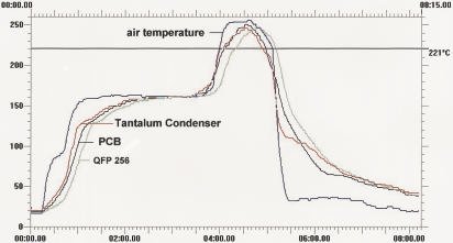
The temperature profile shown in picture 2 can serve as an example for solder paste with a melting point of 217 to 221°C. The profile was recorded in an SMT 460 C furnace. A board with the dimensions of 200 x 300mm, thickness of 1.5mm and 4 layers was selected for the profile. The measuring points were at a PLCC, a minimelf and the upper side of the assembly. Another sensor was attached 10mm above the board in order to precisely log the actual gas temperature. The conveyor speed was set to 0,40m/min. The heaviest component, the PLCC, was heated up to 237°C. The hottest part of the board (the surface) was only 4K hotter. These temperatures could be realized with a gas temperature in the peakzone of only 252°C. Comparable furnaces of competitors need higher temperatures.
Inspection, rework and reliability
The inspection of SnPb solder joints has been continuously developed and optimized, and the guidelines are used for the evaluation of solder joints in all SMT lines. The use of lead-free paste is based on the condition that corresponding lead-free metallization of the board surface and the components is applied, otherwise the mechanical properties of the solder joints will be deteriorated. Therefore, it is necessary to establish other guidelines for the inspection of lead-free paste, where corresponding attributes for good respectively bad solder joints are defined. The shine, the wetting and the geometry of the solder joint have to be carefully inspected. Since X-ray technology is also being used foradvanced packages (BGA, CSP, flip-chip, etc.), the guidelines for interpretation must clearly define the quality of lead-free solder joints.
The presently valid temperatures for rework have to be raised by about 20K to allow proper processing of lead-free solder. Existing tools for repair can be used further after adapting to the parameters. If different alloys for lead-free soldering are established in the market, then corresponding parameters have to be used for an alloy. For more than a decade, NEMIor partners of the IDEALS project (sponsored by Brite-Euram) cope with reliabi-lity checks for lead-free solder joints.Both favored the alloy SnAgCu. The IDEALS partners (such as GEC-Marconi, Philips, Siemens, Multicore, Witmetaal and NMRC) have obtained the following results:
•The lead-free SnAgCu is favorable due to a relatively low melting point
•Most alloys are compatible with many lead-free metallizations of PCB surfaces (Cu, OSP, Sn, Ag, Ni-Au, SnCu HASL)
•Most alloys are compatible with flux of conventional pastes
•By using a modified reflow profile, acceptable wetting can be realized
•Lead-free paste achieves higher reliability than SnPb in thermo-mechanical fatigue examinations
A lead-free solder paste has to meet all requirements in the manufacturing process. Such a paste is determined by the melting point, which is about 40K above the presently used temperatures. Due to the higher temperatures, PCB and components are exposed to higher thermal stress. Efficient full-convection reflow ovens heat up the assemblies to temperatures required by lead-free paste by using gas temperatures that often are lower than presently employed temperatures for lead-containing paste. However, there are also ovens that had to be operated at gas temperatures above 300°C. With these furnaces, the thermal and mechanical stress for the assembly is considerably higher.
EPP 160
Literature
Prismark report on lead-free solder, February 1999
N.C. Lee, Advancing Microelectronics 9/10 1999, p 29ff
B. P. Richards, C. L. Levoguer, C.P. Hunt, National Physical Laboratory, January 1999
Klaus Brodt, SMT-Wertheim, Heat transfer in forced convection reflow soldering systems
Zusammenfassung
Die Einflüsse des Blei-Prozeß’ auf Boardmaterial, Komponenten und wichtige Prozeßschritte wie Pastendruck, Lötvorgang, Rework und Inspektion sind erheblich. Der Blick auf aktuelle Entwicklungen zeigt, daß inzwischen sogar Lötöfen verfügbar sind, die die höheren Bleifrei-Löttemperaturen mit weniger Thermostreß für die Baugruppe erzeugen als ungünstig konzipierte Öfen für den herkömlichen Blei-Zinn-Prozeß mit seinen niedrigeren Löttemperaturen.
Résumé
Les influences du processus au plomb sur la matière constitutive des cartes, sur les composants et sur les principales étapes du processus comme la sérigraphie, le brasage, le rework et l’inspection sont considérables. L’observation des évolutions actuelles révèle qu’il existe aujourd’hui même des fours à braser qui produisent les températures supérieures nécessaires pour le brasage sans plomb avec un stress thermique moindre pour le sous-groupe que les fours moins bien conçus, destinés aux processus conventionnels utilisant le plomb et l’étain avec des températures de brasage plus basses.
Sommario
L’azione del processo al piombo sul materiale dei circuiti integrati, sui componenti e sulle fasi di processo più importanti come lo stampaggio dell’impasto, il processo di brasatura, il rework e l’ispezione è notevole. Osservando gli sviluppi odierni si può notare come siano disponibili anche forni di brasatura capaci di generare le maggiori temperature richieste dal processo con assenza di piombo con una minore sollecitazione termica per il gruppo costruttivo rispetto ai forni tradizionali per il processo con piombo e stagno con le loro minori temperature.
Unsere Webinar-Empfehlung
.png)
Auch dieses Jahr präsentiert Koh Young wieder aktuelle Trends und „State of the Art“ Technologie aus der optischen Inspektion und 3D-Messung auf der Productronica in München. Aber wir alle kennen das Problem voller Terminkalender, Reisebeschränkungen oder fehlender Zeit, um in…
Teilen:


