With a look at modern systems and process solutions for through-hole plating we want to answer users’ vital questions in the PCB commerce: Are the investment decisions in line with upcoming challenges? What can be done to lower costs and increase profits? How can we maintain our competitive edge?
Gerd Linka, Andreas Threbank, Atotech, Berlin, Germany
The development of through-hole plating technology is influenced by trends such as globalization of the PCB business, a pressure for even more economical manufacture, environmental protection, etc. At the beginning, a short look to the the main factors seems very helpful to define positions.
Globalization – PCBs are being manufactured all over the world. For example, Taiwan has become an attractive place to buyers, with an annual production capacity of nearly 8m-sqm. For a good position in worldwide competition, a manufacturer has to analyze the world market and find the right solution in terms of price, quality, costs, etc.
Technology – Years ago, a decision „only“ was necessary on thin or thick copper plating and which type of vertical production system to use. Now, decisions have to aim at the preparation for upcoming challenges. The IPC Technology Roadmap reveals examples of key technologies fulfilling various demands on PCB manufcature. They provide a solid orientation.
Environment – The PCB manufacturers, like all other industries, are faced with the challenge to conform to environmental legislation and work safety regulations. The laws are restricting or banning the use of EDTA and other non-biologically degradable complexing agents, hazardous substances such as formaldehyde, halogenated hydrocarbons or compounds that increase CSB values. German laws, for example, require an investment of approximately 8% of sales revenues in environmental protection. In contrast, the invest- ments in U.K. amount to only 2%.
Productivity – Maintaining a competitive edge involves close investigation of all areas offering even further potential for manufacturing developments. This is not simply a question of increasing yields, it is also a matter of integrating a process while increasing the level of automation. Considerable savings on energy, water and organization costs can be achieved by a move to a horizontal direct plating system.
Costs – Disadvantages of costs, related to a manufacturing site, can be compensated by implementing other production systems and process technologies. Potential cost savings can be achieved for water, energy, material and staff.
Modern process technolgies and manufacturing systems for through-hole plating pave a way to a competitive edge in the PCB manufacture. Users can choose from a wide variety of concepts. But this makes the selection of the most suitable through-hole plating system a complex and time-consuming procedure. The users have to consider the following: technology; pattern, semi panel or panel plating; manufacturing and processing aspects; vertical or horizontal technique; chemical copper or direct plating and (if direct plating) selection of carbon, palladium or conductive polymer systems. Here, we provide an overview on Atotech’s approach to horizontal through-hole plating systems. Customers’ requirements on PCB and production quantities provide a reasonable basis for decisions on method (horizontal or vertical), process engineering and the selection of an appropriate technique.
Technology aspects
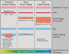
The conductive patterns (semi or full panel plating) for advanced PCBs and components become even more complex. To attain 25µm of copper in the center of a drill hole, the variations in layer thickness for pattern plating range from 40 to 90µm as a result of the layout, and can not be avoided. Combined with soldering masks and a dense SMD lead grid geometry, this drastically increases assembly problems and results in lower yields. This also expands the use of etching solutions for thick copper layers in the plating process.
The semi panel plating provides a viable alternative. After through-hole plating, a surface copper layer of approximately 10 to 15µm is applied. Following exposure, the electrolytic copper is deposited with a thickness of 25µm. This combines the advantages of improved layer density with relatively limited etching of copper layers.
Chemical copper or direct plating and, eventually, the selection of carbon, palladium or conductive polymer layer is another issue. The widely-used through-hole plating process still is electroless copper which deposits the first conductive layer of copper on the laminated material. This is expected to change in the next five years with more companies taking advantage of direct plating. The trend towards it is growing. Especially in Germany there are about 70 to 80% of PCBs produced with a direct plating process.
Through-hole direct plating
The methods currently available for through-hole direct plating can be classified into three groups: palladium, carbon-conductive or polymer-based. To increase conductivity, the tin-stabilized palladium colloid system is brought to react with sulfide ions. This changes copper into copper sulfide. Therefore, the surfaces must be re-cleaned to achieve a secure bond. Because of a high etching rate, the advantages of improved conductivity must be weighted against the sensitivity to wedge or ring voids. In a process where the palladium-tin colloid is brought to react with copper, tin is replaced by copper, and at the same time, the copper surface is cleaned. In a process based on organically stabilized Pd-colloid, this colloid deposited on the copper surface is removed during etch cleaning. This removes 0.5 to 1µm of copper. The process can be used in vertical as well as horizontal systems and is suitable for all base materials. In a carbon-based process, the conductive layer is either carbon or graphite. The process is non-selective. The carbon must be removed from the copper surface to ensure adequate bonding strength of the galvanically deposited copper on the copper backing and the inner layer.
In a conductive polymer-based process, the polymer serves as the conductive layer. This selective process builds up conductive layer only in areas where manganese dioxide has resulted from the reaction of the base material with permanganate. The copper surfaces remain uncoated, which ensures a good bond to the inner layers. A selective process can be used in a variety of simple to complex applications. However, there are limitations in the compatibility with base materials. The PCB manufacturer should make decisions on the most suitable process in close co-operation with customers since time and costs are not wasted if a process will not be approved.
Vertical or horizontal processing
Atotech’s expertise is backed by more than 40 years of experience in the set up of complete fabs through its founding company (Schering). Despite improvements (space-saving conveyor rinsing, vibrators for improved fluid exchange, automated loading and unloading), the vertical process for electrolytic copper plating continues to take a back seat to the horizontal approach.
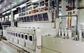
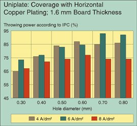
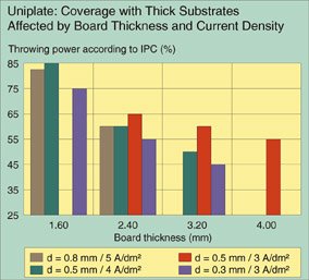
For example, Atotech’s modular Uniplate Cu horizontal system for copper plating features modules with active electrolysis zones in lengths of 3m, 4.5m and 6m. Modules can be combined according to a process, throughput rate, current density and layer thickness. The systems are compact and simplified in the set-up procedure while saving installation costs. A continuous conveyor system facilitates a simple way to automation. Different processes can be integrated, for example, smear removal/through-hole plating/copper plating or through-hole plating/copper plating/photo processing. The horizontal transfer supports the treatment of very thin materials (0.1 mm), standard (1.6 mm) and thick materials with 4mm and more. Guide devices are required for thin materials, the thick ones require other constructions. The PCBs are transported over plastic rollers and are staggered to counterbalance interference of the electrical field.
The electrolyte is sprayed by nozzles to ensure full coating of surface and drill holes. This reduces the diffusion layer thickness on the substrate, which enables medium current densities of 8A/dm2 without scorching the electrodeposit. The electricity is transferred to the PCBs via insulated clips. The clips are transported on a continuous loop conveyor and electrolytically stripped on return. Before entering, the bare PCBs are positioned in an alignment station. The substrate is inserted into the copper plating module in a straight line at a precisely defined distance. This enhances the even distribution of the layer and the electric current. With an diaphragm regulatorboards of different sizes can be processed. Anodes (phosphorus copper pellets) are arranged in retractable, insoluble baskets above and below the PCBs.
Horizontal through-hole plating and copper processing systems have been widely implemented in high-volume shop floors. For example:
• Direct plating with Neopact and 1 Uniplate Cu 6 for through-hole/flash copperplating. The system throughput for 610mm x 460mm blanks at a conveyor speed of 1.6 m/min is 60qm/h.
• Direct plating with Neopact and 2 Uniplate Cu 6 for through-hole/semi panel plating. System throughput for 610 mm x 460 mm blanks at a conveyor speed of 1.2m/min is about 45m2/h.
• Through-hole plating with a throughput for 610mm x 460mm blanks at a conveyor speed of 0.7m/min is 25m2/h.
• Direct plating with Compact CP and 4 Uniplate Cu 6 modules for through-hole/panel plating up to a specific layer thickness. Throughput for 610 mm x 460 mm blanks at a conveyor speed of 1.2 m/min is 45m2/h.
• Telephone card tin/lead plating with Uniplate SnPb6 for telephone cards. The system has a conveyor speed of 1.3 m/min. and a throughput of 50m2/h.
Horizontal systems have been chosen almost exclusively because of the requirements in the manufacture of complex PCBs. In contrast to vertical systems, the horizontal ones offer some benefits – especially for finer structures and smaller drill holes:
• Compact and lightweight, significant savings in terms of space planning and buildings
• Racks are unnecessary, eliminates costs for stripping and maintenance
• Lower number of anodes and anode baskets (insoluble anodes will reduce downtime for maintenance)
• Economic approach for expanding and modifying systems
• Automated loading and unloading
• High-level automation eliminates operation errors
• Reduced requirements for air, water and wastewater treatment
• Improved MTBF and MTTR
Horizontal systems allow for a uncomplicated treatment of thin PCBs down to 0.135mm, and the force-flooding of drill holes ensures good fluid exchange. They provide improved, more even surface layers, and each board is produced under the same controlled condition for a consistent, high-quality result. The surface tolerance is between ±10%. With the trend towards more complex multilayers, the demand for horizontal systems and improved throughput is increasing. Today, 40% of Europe’s major manufacturers are using horizontal production systems for through-hole plating. The hands-on knowledge gained with horizontal through-hole and copper plating systems indicates that high-quality, PCB mass production with a very even metal layer is achievable. This results in a shorter etching and lower costs. More uniform etching leads to consistent widths and heights for conductor strips which is important for impedance-controlled PCBs. The yield for ultra-thin PCBs increases while conductor pattern defects from overetching are reduced. The solder mask lacquer application can be reduced by nearly 30%. Thin substrates can pass horizontal systems without mechanical damage, resulting in increased yield.
Leiterplatten sind zum globalen Geschäft geworden, Consumer-Standardware kommt in großen Volumen aus Asien. Der Druck auf die Preise – und damit auf die Produktionskosten – ist sehr hoch, deshalb müssen alle Möglichkeiten der Optimierung und Automatisierung ausgeschöpft werden. Zudem gibt es Gesetze zum Umweltschutz und Arbeitsschutz, die zwingend zu beachten sind. Innovative Leiterplatten-Technologien in der Durchkontaktierung helfen, im globalen Wettbewerb erfolgreich zu bestehen.
Les cartes de circuits imprimés sont devenues un marché global et les biens de consommation standard viennent d’Asie par grands volumes. La pression exercée sur les prix – et par là même sur les coûts de production – est élevée, et c’est pourquoi toutes les possibilités d’optimisation et d’automatisation doivent être épuisées. En outre, des lois relatives à la protection de l’environnement et à la sécurité du travail doivent être impérativement respectées. Des technologies de cartes de circuits imprimés novatrices lors du montage transversal aident au maintien dans la compétition globale.
Le schede per circuiti stampati sono diventate merce sottoposta alla concorrenza globale, il materiale standard di grande consumo arriva oggi in grandi quantità dall’Asia. La pressione sui prezzi, e dunque sui costi di produzione, è alto, per cui devono essere sfruttate tutte le possibilità in fatto di ottimizzazione e automazione. Inoltre esistono leggi ambientali e antinfortunistiche che devono essere assolutamente rispettate. Le tecnologie di realizzazione di contatti innovative per le schede per circuiti stampati aiutano a sostenere la pressione della concorrenza mondiale.
Unsere Webinar-Empfehlung
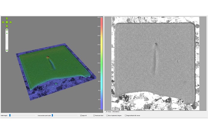
Applikationen aus dem Bereich der Leistungselektronik gewinnen immer mehr an Bedeutung. Die Inspektion dieser Applikation lässt sich mit der bewährten Standardtechnologie der 3D-Messtechnik bewerkstelligen.
Teilen:


