The realization of Bluetooth solutions requires profound product, integrated circuit and substrate design for its optimization while meeting the specifications. We will have a look at the determining factors for cost and size with the implementation of various SIP (system-in-a-package) models. The search for the right solution extends also to substrates where LTCC (low temperature co-fired ceramics), glass and silicon-on-silicon are being used as alternatives.
Douglas J. Mathews, Director,Module Applications Engineering,Amkor Technology
Considerations for packaging
The Bluetooth development is driven to a great extent by the trends towards smaller, lighter portable communications products with cost as a primary momentum. Other possible Bluetooth applications are add-on peripherals for computer equipment, headsets and a plethora of yet to be developed implementations. Many of these solutions do not require the size and cost targets of a cell phone application and can sustain higher prices or larger sizes respectively.
While the commoditization of Bluetooth needs standardization, it is limited by the variations in the implementation and the application. A system application is comprised of software, substrate, chip, mechanical, manufacturing and people. The application can generally be divided into two categories: hosted, where the digital signal processing (DSP) requirements are absorbed by the host processor, and stand-alone, where the DSP is required to operate independent of a host processor. This fragmentation will drive the development of two implementations: one with the DSP included and one without.
IC systems & partitioning
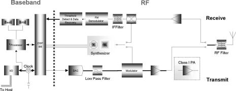
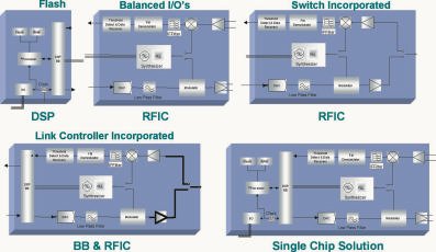
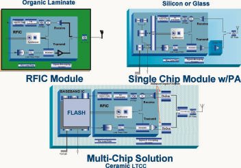
The Bluetooth specification is quite clear on what functionality is required to realize system performance, but there are no constraints as to how it is implemented. IC designers present large variances in how a system is implemented in terms of partitioning. Among the available ICs are RFICs, link controller ICs, microcontrollers, flash, combined RFIC and link controller, and combined single-chip solutions with microcontroller, DSP and RF integrated. The various chips are combined with supporting circuitry in a system-in-a-package (SiP) or module.
A single-chip concept that incorporates the functionality of figure 1 will have advantages in size and cost. However, a single-chip solution is not a straightforward design task with the implementation of digital, mixed signal and RF on the same substrate, nor does it necessarily lend itself well to the best performance and cost tradeoffs. RF CMOS at 0.25em geometry is likely to be able to meet both the cost and performance targets of a class II or III system, while increasing an already lengthy IC design cycle, particularly for the RF portion and its interaction with the baseband block. Bluetooth is a more reasonable wireless specification for utilizing CMOS, and technologies such as SOI, BiCMOS or SiGe BiCMOS are capable of supporting the entire solution set, but at a cost exceeding that of digital CMOS. The realization of digital CMOS is much more cost effective, and the RF technologies are capable of providing the performance required. Therefore, an implementation in more than one chip with varying technologies is evident. Figure 2 depicts several incarnations of IC partitioning.
The implementation of the RF circuitry varies depending upon the architecture and partitioning, and the base semiconductor technology impacts the partitioning. The circuitry can be realized in CMOS, BiCMOS, silicon-on-insulator (SOI), Bi-CMOS, and SiGe BiCMOS. The architecture has to take advantage of the properties of the underlying technology achieving performance and cost efficiency. In most cases, it is not reasonable for all of the RF functionality to be on die. The off-the-die circuitry then becomes one of the primary drivers of cost and size. An IC designer who has been able to incorporate these functions on die gains a distinct advantage in size and cost, depending upon the cost of the die.
Off-the-die circuitry
Off-the-die (OTD) circuitry along with the ICs and their partitioning drives the size and the cost of a SiP. This circuitry is determined by the system architecture, the application and the functional implementation.
Antenna – The antenna, always OTD circuitry, can be a discrete or embedded implementation. Embedded is defined as residing within the substrate structure. Discrete means it is attached to the substrate, for example by solder, epoxy, etc. A wrong antenna can render a product ineffectual. Antennas will affect the system cost and size by the addition of layers to isolate it from the circuitry or by the space required to place it. Antennas will likely exist separate from the SiP. Consultation with a design house is an important aspect.
RF filter – The RF filter can be embedded or discrete, too. An embedded filter is realized by transmission line structures requiring quarter-wavelengths of line length. Multiple layer embedding can reduce the impact of the filter size by taking advantage of the space below the die, but multiple layers add cost. A discrete implementation (with passive components) can also be achieved. In the case of a cellular handset, the transmissions from the phone may not impact the receive sensitivity of the Bluetooth system; hence the filter has to assure that the out-of-band blocking is not influenced.
Switch – Sometimes a switch is used to toggle between receive and transmit, or to change between class I and class II or III operation. Switches can be made up of wire-bondable Pin (P-intrinsic-N) diodes, packaged Pin diodes or integrated switches. Packaged diodes will add to the module size (SOT23 are on the order of 2x3mm). Also, additional biasing lines and passives are required. It would be desirable to use a wire-bonded version. Many are looking for space savings by flip-chip technology. While flip- chip and wirebond can co-exist in a process, the added cost may not be worth the space saved. Some implementations have no switch because Bluetooth is not based on simultaneous transmit and receive.
Power amplifier – For class I operation, an additional power amplifier is required to meet the specification of +20dBm along with RSSI (receive signal strength indicator) and feedback for power ramping. This circuitry can be either realized as another IC or a mix of active and passive discrete and embedded components. A module with class I or III operation can be achieved by a bill-of-material (BOM) and assembly change. The area necessary for the amplifier will increase sizeand cost, but it may be the most flexible way.
Baluns – In many cases, IC designers have implemented a balanced approach to minimize the issues of noise and/or grounding with single-ended circuitry. Since a pair of signals delivers the RF inputs and outputs with 180° phase difference, a balun combines these two out-of-phase signals into a single-ended line. The balun takes additional space, but can be buried within layers. It can be discrete implemented as well, and is subject to variations of substrate, passives and placement.
Synthesizer: The VCO and PLL circuitry is contained in most IC implementations. However, the loop filter is OTD usually consisting of a capacitor and/or resistor. The capacitor may be a critical component requiring temperature compensation and/or high tolerance provisions.
Decoupling and bypass capacitors – Low-frequency bypass and decoupling capacitors are usually large, and not included in the die. Depending on the substrate, it may be implemented as a discrete component. The value required along with the substrate capability will drive the selection of embedded or discrete.
Clock – The crystal is the key element here. It is always OTD and can be quite large. Usually it is located on the product motherboard. However, for stand-alone applications the crystal is likely to be included in the SiP.
Flash – Much of the firmware is still under development, and as the Bluetooth system is expected to undergo further changes, the incorporation of flash memory seems reasonable. Some processes allow for the inclusion of flash in the semiconductor, but sometimes an additional flash chip will be required. Die stacking can help improve the size, but will add cost due to the process.
Assembly methodologyand package type
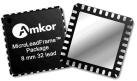
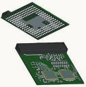
Package type selection is dependent upon the application and the cost and size goals. A RFIC can be implemented either as a packaged part with the motherboard supporting the OTD circuitry or as a module. In the case of a packaged RFIC, the package must provide high-frequency performance. A package such as Amkor’s MLF, depicted in figure 3, would serve high performance requirements. The key is maintaining short wirebonds and lead lengths to minimize inductance as well as providing a very good ground for the RFIC.
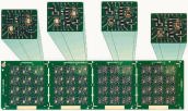
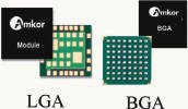
For modular applications, the package style generally falls into one of two categories: land grid array (LGA) or ball grid array (BGA). Both utilize a strip format for high-volume manufacturing (figure 4). The package dimensions will impact the overall cost of a module. Ideally, it should be optimized to fit into the strip for a maximum number of units, hence reducing cost. The primary difference between LGA and BGA is the method of connection to the motherboard. The LGA utilizes land areas for the I/O connections that are soldered to the mainboard, while in a BGA an array of solder balls is used. The number of connections and customers‘ preference drives the method used. Ball attachment is an additional cost, and requires routing of signals and ground to a location within the array which can impact cost and performance. Figure 5 is a representation of both styles.
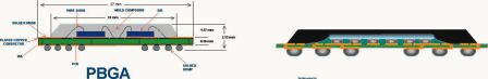
BGAs can be realized in a variety of formats and substrates. For example, PBGA packages are encapsulated with a plastic overmold (figure 5). While providing protection, the overmold can impact the RF performance. As with any RF/microwave circuitry, a dielectric layer changes the transmission line impedances. PBGAs, normally wire-bonded, can also be manufactured using flip-chip technology. With flip-chip-on-laminate, underfilling is required to deal with the differences in temperature coefficients of expansion between laminate and silicon. Like overmold, the additional dielectric can impact the performance. It is widely believed that flip-chip assembly will reduce the size of a circuitry. However, additional space is required to allow for the underfill nozzle to be placed in close proximity to the die. Depending upon the interconnect scheme, routing of signals from under the die can present problems. Designers must take care not to space flip-chip attach points so close as to present manufacturing problems and restrict routing of signals. Cross sectionsof the FC-BGA and PBGA are shown in figure 6.
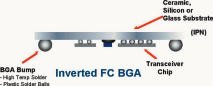
For packages a variety of substrates are used including ceramic, glass and silicon. Ceramics are utilizing low temperature co-fired ceramics (LTCC); also glass is beginning to be used. Ceramic circuits can be realized both as LGA and BGA, and like glass and silicon, ceramics can also be configured as inverted BGAs (figure 7). An inverted BGA is generally required for glass and silicon modules due to the lack of through-hole capability in the substrate. LTCC may use this when it is desired to have an antenna embedded in the ceramic on one side with the interconnections on the other. One limiting factor is that the overall height of any component cannot exceed the height of the solder balls, once reflowed. This can create issues for larger discretes, or require that an opening be put into the board to accommodate those components.
With a flash memory within the module and functionality requiring both RFICs and DSP chips, the size can begin to grow rapidly. If flash is not containable within the DSP, this chip can be stacked upon the flash memory (figure 8) or vice versa. For Bluetooth, memory requirements are generally much more size-intensive than the DSP.
Test considerations
For the full implementation of the Bluetooth standard, electrical tests are well defined. Special test modes are given by the Link Management Protocol that allow the UUT to be put into a loopback mode to allow detailed tests of the RF and baseband functionality. These modes will allow conformance testing of burst timing and drift, bit error rate, dynamic receiver range and power control of the transmitter (if applicable). If a SiP encompasses only the baseband and RF sections, tests become more complicated, since the equipment must then provide all control signals and protocols.
For production tests, the interface between the UUT and the tester will be critical. For high-volume manufacturing, high throughput, automated handling equipment will be a condition. The amount of metal in the immediate vicinity of the module must be minimized to reduce the impact from a fields and waves perspective. The contacts between the module and the load board must be a RF low-inductance type, with paths as short as possible. The impedance of the RF lines must be carefully controlled to avoid power being reflected back. Care must be taken on the analog and digital lines as well to avoid introducing noise.
Bluetooth modules are being configured both with packaged die and bare die. The packaged-die case takes advantage of its testability; the disadvantage is the additional size and cost. For the bare die, testing becomes problematic due to the need to wafer probing. Bare die bring up the issue of known-good-die (KGD).
Single-chip and multi-chip solutions
The variance of the implementations is high not only in the ICs themselves, but also in the substrates. The units are realized as RFIC modules, link controller and RFIC, single-chip and with flash. In addition to the variation in ICs, substrate implementations include laminates, LTCC and glass. It is foreseeable also that lower cost laminates with IPN (integrated passive networks), such as glass and silicon, for the key implementations are likely to occur. Various versions of SiPs are depicted in figure 9.
Two-layer laminates are the least expensive substrate solution for a module in a given size, but it is likely to be the larger with more variance. The Bluetooth specification is very forgiving and can accommodate a large amount of variation. Induced variance will be dependent upon the OTD circuitry. The greater the integration level of the RF the more likely laminates maybe a successful choice. Even in the case where OTD circuitry is required, multi-layer laminates may provide an alternative, despite additional cost.
The cost efficiency of LTCC is based on embedded passives within multiple layers of ceramic. Glass is gaining popularity, though high-volume production has yet to be achieved (about 250K units/week). Glass and silicon are being used as IPN substrates where a variety of capacitors, resistors and planar inductors are being realized in a smaller space and with less variance. Both require either wirebonding the substrate to another substrate or inverted BGA implementation. In the case of inverted BGA, the balls are routed to the outside of the substrate thus increasing size.
Physical model
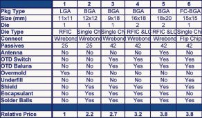
For illustrating the impact of various implementations, we used a physical model of a laminate Bluetooth system. In a pricing analysis, several parameters were varied, and the overall price of a SiP was examined relative to a simple one-chip module. One variation of the model (number 5) is shown in figure 10. In this solution, a baseband processor and RFIC are implemented in a BT laminate, 2-layer substrate (2 metal, 1 dielectric core) BGA. The larger rectangular area represents a surface-mounted antenna. The SiP also incorporates discrete passives for filter and the baluns as well as wire-bonded Pin switch diodes. This implementation resulted in an 18x20mm module that has not been optimized for size. Pricing has been referenced to the least costly implementation of this particular substrate type. Table I depicts multiple solutions and relative pricing, with constants of the following: high-volume rates at 250K/week; BT resin substrate; 2-layer and discrete filter. Pricing is exclusive of die cost and test yield.
System 1 is comprised of an RFIC with external circuitry (discrete filter, loop filter and decoupling and bypass capacitors). It is realized as an LGA and with wire bonding. System 2 is a single-chip solution incorporating RFIC and DSP, with the same OTD circuitry as in #1, but in a BGA format. The most significant difference in the cost (aside from the die) is the addition of encapsulant, solder balls and space required for the attachment of a shield. The relative cost is 2.2-times higher than that of system 1, though roughly the same size and die count.
System 3 is also a single-chip solution (as configuration #2), but with the incorporation of baluns and switch, and the module size has increased by the OTD circuitry. The cost is slightly higher than #2, primarily from the growth of the substrate and passive incorporation. System 4 is the same as #3, except that it is a two-chip solution. Additional space is required for the secondary die, interconnects to the RFIC and decoupling and bypass capacitors. Again the size has grown and the price as well. System 5 is the same as #4, with the addition of a surface-mounted antenna. The cost has grown to 3.8-times that of system 1.
As a single-chip solution with a flip-chiped die and packaged switch diodes system 6 is fairly different. The size of the package has decreased notably, but not proportionally, and is roughly the same cost as the larger #5. The price is driven both by process and size. Flip-chip is more costly and requires underfill to deal with the differences in the temperature coefficients. The size of the substrate could be smaller, but for the underfill some space around the die is required, allowing material application through a nozzle. The sizeof the substrate could be decreased with wire-bondable diodes. While flip-chip and wirebond may exist within a single process, the result is more costly. A tradeoff of processes, component selection and size considerations could minimize the cost. While this example was for BT resin, the matrix of complexity increases for every substrate examined.
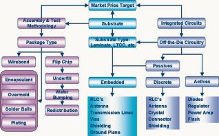
In order to achieve the price target fora application not only must the designer consider the implementation of the IC, but alsothe substrate, OTD circuitry, assembly and test method. Figure 11 summarizes many of the major cost contri-butors. All components of the flow-chart can affect performance as well. A solid understanding of the cost variables and their effects on performance and size is needed.
IC and SiP level will impact the cost of a system. It is essential that the package be considered up front, preferably as the die is being designed, or the potential for increased costs likely will surface. System and IC partitioning, substrate selection, passive implementation, assembly and test methodology are the major contributors of system cost.
Co-design of asystems level solution
The most effective way for optimization is by concurrent engineering or co-design. Co-design realizes that systems engineering is required at all levels: product, IC and substrate. In co-design it is recognized that the package is a functional part of a Bluetooth system. For optimum cost and size the package must be designed in parallel and interactively with the IC and product designers. Simulations are shared to insure the functionality required. An understanding of manufacturing processes, production test and design decision impacts are key for optimization. Supply-chain management must also be considered, with the need to source and second source all the components. To bring multiple companies together in a co-design effort, program management is required.
Amkor Technology has implemented a program of enabling Bluetooth and other wireless systems through co-design. With a full complement, ranging from systems to component engineering, our design staff bring package and substrate design to fruition in a shorter cycle time. With the understanding of manufacturing processes, their impacts and capacity installed, the ability to meet the costs is in place. Additionally, Amkor has begun the implementation of RF test both at the die and module level. With our established digital and mixed-signal capability, we are offering all-inclusive systems.
The dominating element of cost is the die itself. An evolution of the many implementations will be necessary to arrive at the lowest die cost. Host and stand-alone applications are driving Bluetooth RFIC and DSP/RF modules. This segmentation will likely further be enhanced. Alternative substrates will be used. Flexible films, silicon and glass are likely candidates, but cost reduction, optimized assembly methods and high-volumes will be required.
EPP 173
Zusammenfassung
Der „Blauzahn“ ist derzeit als kommende Technik zur Anbindung von Peripheriegeräten an Rechner oder als kurze lokale Kommunikationsstrecke hochfavorisiert. Noch aber ist Bluetooth weder vollständig standardisiert, noch geklärt, wo alle herausragenden Anwendungsvorteile im Detail liegen dürften. Das heißt für die Realisierung und damit auch das Baustein-Packaging, sehr flexible Lösungen sind Pflicht, damit sowohl technische Entwicklungen problemlos verfolgbar sind, als auch die Kosten für hochvolumige Applikationen niedrig gehalten werden. Die momentane Zielvorstellung für Bluetooth-Implementationen liegt bei circa 2 Euro.
Résumé
La „dent bleue“ est une technique actuellement considérée comme hautement favorite pour le raccordement de périphériques aux ordinateurs ou pour la réalisation de circuits de communication locaux courts. Mais le Bluetooth n’est pour l’instant pas entièrement standardisé et on ne connaît pas encore dans le détail tous les avantages majeurs de son utilisation. Autrement dit, des solutions de grande flexibilité sont obligatoires pour la réalisation, donc également pour le conditionnement des composants, pour qu’il soit possible d’une part de suivre sans difficultés les évolutions techniques et d’autre part de maintenir les coûts à un niveau réduit pour les applications en grandes quantités. L’objectif actuel pour la mise en œuvre de Bluetooth se situe à environ 2 euros.
Sommario
Il „dente blu“ è oggi la tecnica con le migliori prospettive di divenire in futuro determinante per il collegamento di periferiche al calcolatore o per la creazioni di brevi linee di comunicazione. Per ora, però, Bluetooth non è né completamente standardizzato, né é stato ancora chiarito quali siano i veri e propri eccezionali vantaggi di applicazione. Ciò significa che per le soluzioni sia di realizzazione che di packaging dei moduli è richiesta la massima flessibilità, in maniera da poter sia adattarsi senza problemi alla continua evoluzione che mantenere bassi i costi anche in caso di applicazioni ad alto volume. Attualmente l’obiettivo per le implementazioni Bluetooth è di ca. 2 Euro.
Unsere Webinar-Empfehlung

14.05.24 | 10:00 Uhr |
Egal ob serielle Flashes (eMMC, I²C, SPI), parallele Flashes (NAND, NOR) oder komplexe Bausteine (Prozessor, Controller, FPGA, CPLD). Erfahren Sie mehr über den FlashFOX als innovative Lösung zur Embedded In-System-Programmierung elektronischer Baugruppen…
Teilen:


