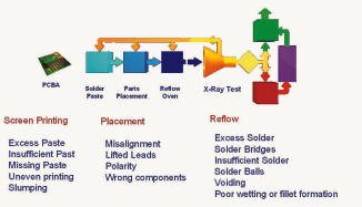
Mobile electronic products are continuously getting smaller in conjunction with increased functionality. This leads to very complex manufacturing issues, especially for SMT-based assemblies. In the field of inspection, the application of X-ray technique (AXI) has advantages in detecting certain production-related defects in a reliable way. Also, AOI is able to find print and soldering-based faults. Here we try to clarify a bit when to use these different technologies.
Dino Franz,Macrotron Process Technologies, Munich
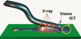
Conventional verification methods such as in-circuit (ICT), boundary-scan or functional tests can only be partially applied because of limited test access. Contact-less techniques for structural testing need to be increasingly used if product quality has to be verified. In SMT lines, two techniques are standard: automated optical inspection (AOI), and automated X-ray inspection (AXI). Both methods have their advantages in detecting certain defect types, whereas AXI is the most reliable technique. AXI is able to detect those defect types that occur in SMT production. Because these systems are providing true measurements, a sensible process control is possible.
Where are defects introduced?
Figure 1 shows the principle of an SMT production line that includes a test system. Every single production step is able to and definitely will eventually introduce defects to the process, independent of the quality of each step. Defects can neverbe totally eliminated, but with the ap-propriate test equipment, the sources canbe identified and therefore the defect ratecan be minimized to only a few ppm.
The stencil print and reflow processes can create soldering-related defects, and the pick&place machine will create solder joint-related as well as component-related defects. Studies have revealed that more than 70% of all flaws on a typical SMT board are solder joint-related defects, the majority caused by the printer and a small portion from the oven. When the boards become even more complex, this percentage is prone to rise remarkably. The manufacturer tests components, and, therefore, in board assembly there is normally no big influence from this side. However, the quality of solder joints lies surely in the responsibility of the board assembler. Their quality represents very much the SMT production process. It is obvious that an effective process control is directly related to monitoring the quality of solder joints.
Before defining the best inspection concept, two questions need to be clarified: where and what to inspect? Preferably, an inspection system is applied directly after each production step. As this will definitely give the best results, it might not be very cost effective. So, a strategy that offers the best cost-performance relation is very important.
Paste inspection by AOI systems
The stencil print is still one of the main causes of soldering defects. The idea is to check very closely here for good print quality. Some highend printers have already built-in AOI systems. However, their mechanics are designed for a good quality print and not for fast inspection. Hence, 100% inspection is impossible if high throughput has to be maintained. This means only sample inspection is possible, in the hope that those samples represent the overall quality, and gather enough data for an effective process control. In reality, the expensive AOI option of a screen printer is often unused, especially in high-speed assembly lines as those sample inspection cycles reduce the throughput remarkably.
If paste inspection is the way to go,a dedicated AOI system is necessary. Mactrotron’s MVS-1B is specifically designed to reliably inspect paste prints for any possible defects, in 2D as well in 3D mode. AOI systems have proven in the field that they are perfectly suited for paste print inspection. The false call rate here is extremely low as inspecting paste print means mainly verifying an area of homogeneity which is a very reliable procedure.
What about AXI at this point? Theoretically, an X-ray system would be an appropriate solution to detect paste print defects. Some years ago, Macrotron and NIS examined the use of X-ray technology here, and found that the advantages can lead to very good results. AXI always gives 3D information of the solder print, as the height of the paste changes the absorption of X-rays results in different gray levels. The fact that this technology is not used in production yet is only based on the price differences between AOI and AXI. When X-ray technology becomes a wide spread standard, investments will certainly drop, and this method may serve as an attractive alternative.
Component inspectionprior to reflow
If it is necessary to verify reliability and accuracy of a pick&place system, the inspection step directly before the reflow oven seems ideal. Any self-centering effects provided by the reflow process which would influence the results, then do not play a role. Obviously, AOI has some advantages here compared to AXI. AOI systems like the MVS-2B checks for the proper components, accurate placement and right polarity. At the surface of many components, the marks can be read to ensure that the correct components are placed. AXI systems suffer here from the fact that many materials (as plastic packages) do not absorb X-ray very well, and, therefore, appear invisible on the screen which makes an effective inspection impractical.
Post-solder inspection
Somehow at the end of the SMT line, testing needs to be performed to ensure to catch as many defects as possible independently of the process steps where they are created in the assembly line. AOI and AXI systems struggle here for the solution of which technology provides the most reliable and most effective inspection?
Back to the open question, what is to be inspected? On SMT boards we find three different package types in principle: chip style, leaded versions and area-array components. The ability to find defects depends heavily on the package type for AOI or AXI technology, respectively.
Area-array components
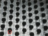
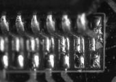
Let’s start with the latest type, the area-array components. This category consists mainly of ball-grid arrays (BGAs), chip-scale packages (CSPs) and flip-chips. All of them have in common that the body of the component covers the connections. This is prohibitive in using an AOI system, as in this case it can only check for the presence of the component. An AXI system (GenRad/NIS CXI-3600 or MV-6100) is capable of looking through the semiconductor, and inspects every single solder joint. The solder balls absorb X-ray far more than any other material, resulting in a good-contrast image. Figure 2 shows BGA balls in an oblique view. Note that the bottom side of each ball is not sufficiently soldered to the pad. Maybe the electrical connections are valid, and an ICT might check this as a ‘passing’ board. But this assembly definitely will fail in the field, afterwards.
Defects that are more obvious such as shorts or opens are also easily detected by AXI systems, even in a perpendicular view. AOI systems will fail here. As area-array components are increasingly used, an X-ray system is essential to verify the interconnection quality under these components.
Chip components
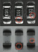
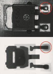
To the category of chip components belong tiny capacitors and resistors, among others. The solder joints at chip components show a fillet shape with a defined slope. These joints are normally visible and can, therefore, be inspected by AOI. The only information available for AOI technology here is the reflection of the material. Hence, the surface of solder joints affects the result of the inspection. The color of the PCB has a similar influence on the inspection. X-ray inspection systems are not affected by those influences, as only the absorption factors of the materials count. In figure 3 there are chip resistors shown as optical and X-ray images. While the solder joints can be recognized clearly, defect types can occur that are not optically visible. The chip in the middle has some porosity in the solder joint, and the right chip has solder balls beneath the body. Such effects can only be seen by X-ray imaging. Solder balls can be very critical, since vibrations transport them and they might cause shorts at components.
Leaded components
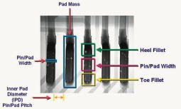
Parts with leads traditionally are available in the greatest variety of package types, such as SOT, SO, QFP, PLCC and many more. Common to those components is the fact that a big portion of the solder joint is always hidden by the lead itself. At gull wing-shaped leads we can, in principle, separate four sections of a solder joint: toe fillet, side fillet, heel fillet and the solder between lead and pad (figure 4). Only the toe and the side fillets can be inspected by AOI as those are visible. The solder between lead and pad is definitely invisible for every AOI system, and therefore any porosity in the solder layer is not detected. The biggest amount of solder runs along the heel of the lead (figure 5). This means, the heel fillet provides the necessarily firm mechanical connection between lead and pad. Only an inspection system that is able to check the heel fillet can verify whether these components may work in the assembly reliably for years.
Some AOI systems use oblique cameras to look at an angle between the leads to observe at least a small section of the heel fillet. This is possible for some SOICs that have a pitch from 50mil or bigger. If the pitch is smaller – which becomes standard in SMT – there is no angle that allows inspection of the heel fillet with AOI, since the neighboring leads are covering this section. As figure 6 shows, only the outer leads may be inspected this way. Even when the side and toe fillet images are available, the difference in an optical image for a good or a bad solder joint is so small that there is probably a high chance that this AOI system might miss the defect. Figure 7 shows an SOT as optical and X-ray images. While in the optical image the defect is almost not to be discovered, in the X-ray image it is apparent. If an AOI systems needs to be able to detect almost the same number of defects as an AXI system, it needs to be tuned with very tight limits, so even many of good solder joints will falsely be detected as bad. Therefore, AOI systems for post-solder inspection have remarkably high false call rates, which makes them in some circumstances unusable.
An SOT package is soldered with the cooling plate to the pad. In many cases, the copper layer of the PCB acts as a heat sink. It is essential that the whole plate is soldered to the pad with no or only very little voiding. Figure 7 reveals that only 80% from the plate is soldered, and some voids are evident. That information is hidden for any AOI system.
Components with J-leads such as PLCC and SOP normally expose two heel fillets. The outer heel fillet can somehow be inspected with the oblique camera of an AOI system. The inner heel fillet is totally covered by the component, and therefore only inspectable by AXI. Some critical applications might require that both sides of the lead are proper soldered. To ensure this, an X-ray system is essential in such a case.
Process control
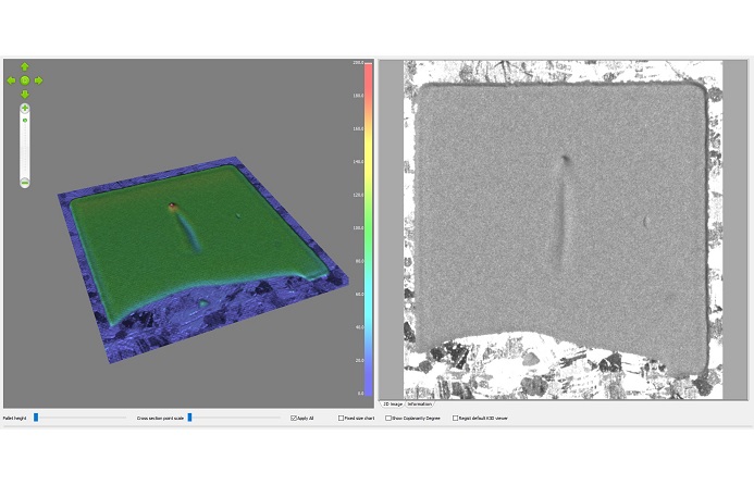
The detection of possible defects is one issue in SMT production. This helps to guarantee (after rework) that the final product works reliably in the application designed for. The other issue is process control which mainly means to reduce the number of defects occurring. Only an effective control is able to achieve this. Process control increases its efficiency the more data are available from inspection. The AXI systems CXI-3600 and MV-6100 are able to supply 30 measurements for each solder joint. Moreover, these measurements are very precise. Measurements related to solder amount provide data for the quality of the print and reflow processes. Distance measurements to verify the side fillet give information of the accuracy of the pick&place systems. A combination of these measurements gives very accurate information not only of the presence of a defect, but also of the type and cause of defects. The statistic tool X-Stat illustrates distribution of the defects in a layout viewer. The defect cause is visualized by means of different colors, to easily locate the point where defects are introduced.
For the visualization of the measurement data, we use the on-line monitoring tool X-Mon that is part of the SPC package X-Pert solution, too. The data are shown either as time-dependent graph or as a distribution. The time-dependent graph can show tendencies of measurements, and therefore process fluctuations are observable. This means, defects can be avoided before they occur. If the printer does not apply enough paste onto the PCB, the amount of solder is not sufficient for a stable process. The graph generated by X-Mon will move towards a lower warning limit. When it reaches the limit, a warning message appears. Immediate action can be provided, and the process turns back to normal. In this way, there was no raise of the defect rate to note. If an AOI systems supplies only three to four measurements per solder joint with restricted accuracy, it is almost impossible to perform an effective process control.
Many obscured solder joints can only be inspected by AXI systems. With all the upcoming advanced packages, this trend will surely continue. First-pass quality is a prerequisite, since assemblies with advanced packages are very difficult to repair. AXI equipment adds value, because with appropriate tools for statistics they provide the necessary data for efficient process control. The production-based defect rate can be minimized, staying low, and this justifies the investment very quickly.
EPP 193
Zusammenfassung
Sowohl die optische (AOI) als auch die Röntgeninspektion (AXI) haben mittlerweile ihrenfesten Platz in der Qualitätssicherung der Baugruppenfertigung. Die optische Inspektion basiert auf demdirekten visuellen Erfassen von Merkmalen auf dem Board. Mit der Röntgentechnik können zudem auch noch Bereiche unter Bauelementen sorgfältig inspiziert werden. Allerdings sind für AXI-Systeme im allgemeinen auch höhere Investments nötig als für AOI-Konfigurationen. Wo also liegen in der Anwendung die Vor- und Nachteile beider Techniken?
Résumé
L’inspection optique (AOI) et l’inspection par rayons X (AXI) se sont toutes deux imposées dans l’assurance qualité de la fabrication d’ensembles. L’inspection optique est basée sur la reconnaissance visuelle directe de caractéristiques sur la carte. La technique des rayons X permet d’inspecter également de manière approfondie des zones situées sous les éléments. Mais les systèmes AXI exigent généralement des investissements plus élevés que les configurations AOI. Quels sont par conséquent les avantages et les inconvénients de l’application des deux techniques?
Sommario
Sia l’ispezione ottica (AOI) che l’ispezione Röntgen (AXI) ricoprono un ruolo stabile nell’ambito dell’assicurazione della qualità di impianti di produzione di gruppi costruttivi. L’ispezione ottica si basa sulla diretta rilevazione visiva di caratteristiche sul Board. Con la tecnica Röntgen possono inoltre essere ispezionate anche le zone al di sotto di componenti costruttivi. Va però detto che per sistemi AXI in generale sono necessari investimenti superiori rispetto a configurazioni AOI. Quali sono dunque dal lato pratico i vantaggi e gli svantaggi delle due tecniche?
Unsere Webinar-Empfehlung
Applikationen aus dem Bereich der Leistungselektronik gewinnen immer mehr an Bedeutung. Die Inspektion dieser Applikation lässt sich mit der bewährten Standardtechnologie der 3D-Messtechnik bewerkstelligen.
Teilen:


