Carbon-conductive inks provide a low-cost method of applying conductors and resistors to base materials and ceramics by screen-printing. These inks can substitute gold, or serve as resistors, cross-over conductors or shields.
Rüdiger Dietrich, Lackwerke Peters, Germany
In the PCB industry, permanent cost-saving is a prerequisite. PCBs produced in medium and large series are mainly used in consumer electronics, and are subject to great price pressure. Therefore, cost-saving in the production is one of the decisive factors in being competitive. Costs can be saved by replacing expensive raw materials by more economical ones and by a simplification of the process. Carbon-conductive inks in the PCB manufacture combines both issues.
The substitution of gold on contact areas reduces material costs remarkably and simplifies handling. When double-sided, plated-through hole PCBs are replaced by single-sided PCBs with cross-over carbon conductors, the savings are even higher. Besides the reduced cost of wet processing during through-hole plating, also the separate treatment of two PCB sides can be disregarded. Single-sided base material can be used instead of the double-sided copper-clad material.
Ink’s fundamentals
Carbon-conductive ink consists of one or more binding agents (polymers), solvents and fillers or pigments, respectively. In the lacquer production the solid ingredients are dispersed into the liquid by a high-speed agitator to dissolve them finely and evenly. After the application of an ink, the solvents evaporate, and following a curing, a polymer film remains on the substrate with the homogeneously embedded solids. For a conductive layer, conducting substances have to be integrated into the ink. The concentration of these substances must be such that a contact of the individual particles or a particle distance of >10nm, respectively, provides a current within the ink. The maximum concentration is mainly dependent on the particles‘ structure and surface. So many solids may be added as can be homogeneously embedded into the polymer. This is the only method of achieving a firmly adhesive, non-porous and close lacquer coating. Metal or precious-metal or carbon powder only can be used as conducting particles. Compared to carbon powders, metals or precious-metal powders yield conductance that is higher by about three tenth powers. This is mainly due to the higher specific conductivity of metal, but also to the smaller specific surface of metallic powder so that higher concentrations in the lacquer are possible. On the other hand, metal or precious-metal powders entail the problems of oxidation, corrosion and migration, and the price of precious-metal powders raises the costs. In its elementary form, carbon occurs as mono-crystalline diamond or crystallized in stratified layers as graphite. Decomposition or organic matter with the exclusion of air or incomplete combustion results in carbon in a third amorphous form, either in coarse masses as coal or in finest dispersion as carbon-black (soot).
The character of soot is determined by the surface and the structure. The specific surface of 80 to 1,200m2/g decides the percentage amount of soot to be used. The structure is determined by the coalescence of the primary particles during the production, and is one of the decisive factors for the necessary density in the lacquer coating. Since soot is produced synthetically, structure and specific surface can easily be controlled during the process. On account of the more amorphous structure, however, an adequate packing density cannot be obtained with soot alone, so that graphite with a more stratified structure is added. The combination results in conductive ink that meets the requirements in the cured lacquer coating. Resistance values of 20Ohm/cm2 can be obtained.
Application examples
Carbon-conductive ink can be employed for the discharge of static electricity from plastics and other insulators. An ink for this application must have good adhesion on the substrate, adequate elasticity, as well as high abrasion resistance. In the PCB industry, the ink can be used for various applications. A partial gold plating on PCBs is mainly effected for the protection of contact areas from mechanical and chemical attacks, to achieve a long service life. With tip contacts, the use of carbon ink will eliminate gold plating and provide substantial savings because the complete plating process becomes obsolete. If a tip contact is made by carbon, it will be sufficient to overprint the contact area with the ink and to protect the rest of the PCB with solder resist.
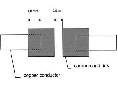
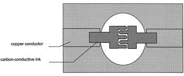
Tip contacts produced by carbon ink are safely protected from environmental influences and corrosion and ensure a safe contacting. The German Federal Post Administration indicates a load of 1,000,000 contacts. Tests have proved that the tip contacts are capable of more than 25,000,000 cycles, which is equivalent to a life expectation of over 100 years. It must be ensured that the metal area provided as tip contact is completely covered with the ink to avoid corrosion and thus contacting problems. This requires a high printing precision level, which can even be substantially simplified by printing onto the base material, using carbon ink only. In the artwork, the conductor is routed close to the contact into an area that will be covered with solder resist later. From this point, the conductor is routed on as ink print, and the contact is ink printed. This simplified process offers some benefits: compared to copper contacts, the printing precision level does not have to be such a high one, and the contact areas are safely covered by a solder resist insulation. The use of carbon ink as an etch resist is an alternative. In this process, the entire conductive pattern including the contact areas are printed on copper-clad base material. The non-coated copper is removed and a finished PCB with ink-protected conductors and contact areas is available. Gold connectors on PCBs can be replaced by carbon. The number of insertion cycles is dependent on the coordination between the spring loaded contacts and the carbon surface. About 20 cycles are possible.
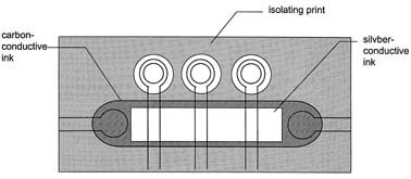
The application of carbon ink, which shows the greatest cost-savings, is the production of cross-over conductors. This process, called CCP (crossover conductive paint), replaces double-sided, plated-through holes with carbon contacts. Here, a single-sided copper PCB gets a contact area at the interconnection points to the next layer, instead of hole and plated-through hole method. The board is then insulated by a lacquer (for instance solder resist), with the exception of the tip contacts and the contacting area. It has to be ensured that the insulation print is absolutely non-porous and the edges of the copper conductors are covered. Depending on conductor design, the solder resist may have to be printed twice with an intermediate drying cycle. To achieve a safe edge covering, base material with 17.5µm copper is normally used because protection is thus ensured more easily.
In the next step, the carbon ink is printed onto the solder resist between the corresponding contacting areas. Then another insulation print over the cross-over carbon conductors and the contacting areas follows. Finally, the tip contacts can be protected by a peelable resist. The conductivity of carbon ink is not as high as that of copper, of course. Thus, the conductor length is limited. There are possibilities to produce longer conductors. Cross-over conductors can be produced with silver-conductive ink instead of carbon. On account of the lower resistance of silver, much longer conductors can be printed. The use of such an ink, however, entails the problem of silver migration: voltage and increased air humidity result in a silver movement that may lead to shorts. This problem may be solved with the printing of silver ink over the insulation lacquer as a cross-over conductor. Contrary to the carbon process, the silver conductor is not routed onto the contacting area, but ends just short off the contacting area. A wide carbon conductor is then printed over the silver and contacting area. Because of the low resistance of the silver, a longer cross-over conductor can be selected, and the complete covering of the silver conductor with carbon ink eliminates migration. The higher resistance of the carbon ink must be considered only for the areas between silver and contacting area.
Processing
When processing carbon inks, attention must be paid to some parameters to ensure that the specified resistance will be achieved. Applying carbon ink by screen printing: the ink is usually highly thixotropic. To achieve the viscosity necessary, the ink must be carefully mixed prior to application. After mixing, a significant reduction in viscosity ensures easy printing. If the ink is left to stand, its thixotropy will increase again. Therefore, it is recommended to remix the ink after longer breaks.
The conductivity of a carbon ink is dependent on the overall cross-section of the conductor (width x height). The resistivity is related to a coating thickness of 25 to 30µm. Very often a compromise has to be found between thickness and desired definition because the finer the selected screen fabric, the better the definition and the identification of details. The coating thickness, however, decreases. The compromise depends on the actual application. Generally, printing should always be as coarse-meshed as possible because the thicker the ink coat, the lower the resistance and the more non-porous and dense the film.
The conductivity of a carbon ink not only depends on the screen fabrics but also on its solid contents. The solid contents indicates which percentage by weight of the ink remains on the PCB after drying. This value is decisive for the properties of the ink and is therefore specified. The solid contents of the lacquer can be modified by adding thinner. The more thinner is added, the lower the solids content and also the coating thickness of the dried ink. This will increase the resistance.
Mixing with insulating paste
There are two reasons for diluting the ink in the production cycle. When changing from a coarse to a finer screen fabric, the ink normally has to be diluted a little to ensure a good printing of details. Attention must be paid that not only the finer screen fabric but also the dilution is resulting in a thinner ink coat and thus a higher resistance. The theoretical resistance must be compared with the actual resistance. A screen-printing ink has to be diluted during a production process because the viscosity has been increased by the evaporation of solvents on the screen. This dilution normally does not create any problems because merely the evaporated amount of solvent is added. Thinning agent should be added in a controlled manner using a viscometer until a specified value is reached.
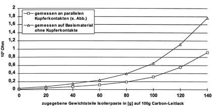
To achieve higher resistance values, some carbon-conductive inks can be adjusted by blending with insulating paste. Such admixing can be realized in any ratio so that a specific increase in resistance can be achieved. In many PCB productions, the boards are placed in stackers and then cured together. Attention must be paid that, at the beginning, the temperature of the oven drops considerably and the cold mass charge has to be heated up. As the curing time relates to the temperature, the heat-up period has to be added. The oven will be back at curing temperature in about 10-min after stacker feeding. It should be ensured that carbon ink will not cured together with two-pack epoxy resin inks (solder resists) in an oven. During the curing, by-products may be released from the epoxy that delay the curing of the ink and may result in a resistance change.
Besides good mechanical properties, a carbon-conductive ink also has very good chemical resistance. Even if chemicals do not attack the conductive ink film, substances may diffuse into the ink and increase the electrical resistance
Mit Carbon-Leitlacken können Leiterbahnen und Widerstände auf Kunststoffe, klassischen Basismaterialien oder Keramik gedruckt werden. Mit Leitlacken läßt sich Gold ersetzen, lassen sich Leitungskreuzungen auf PCBs oder Abschirmungen herstellen oder Widerstände drucken. Durch den Ersatz des Edelmetalls und die vereinfachte Prozeßführung können Produktionskosten minimiert werden. Unter bestimmten Umständen lassen sich doppelseitige Boards durch einseitige ersetzen.
Des vernis conducteurs au carbone permettent d’imprimer des pistes de circuit imprimé et des résistances sur des plastiques, des matériaux de base classiques ou de la céramique. Les vernis conducteurs permettent de remplacer l’or, de créer des croisements de ligne sur des carte à circuits imprimés ou des blindages ou d’imprimer des résistances. La substitution du métal précieux et la simplification du processus engendrent des diminutions considérables des coûts de production. Dans certaines conditions, il est même possible de remplacer des cartes double face par des cartes simple face.
Con le vernici conduttrici Carbon è possibile stampare su materiale plastico, materiali di base classici oppure ceramica dei circuiti o delle resistenze. Con le vernici conduttrici è possibile sostituire l’oro, realizzare incroci di linee su circuiti stampati oppure schermature oppure stampare resistenze. Grazie alla sostituzione del metallo nobile e alla maggiore semplicità del processo è possibile ridurre notevolmente i costi di produzione. Sotto certe condizioni è possibile pure sostituire circuiti a due facce con circuiti ad una faccia.
Unsere Webinar-Empfehlung
10.10.22 | 10:00 Uhr | Conformal Coating ist ein wichtiges Verfahren, um elektronische Baugruppen vor dem vorzeitigen Ausfall zu schützen. Damit bekommt der Beschichtungsprozess eine immer höhere Bedeutung. Dabei ist die Auftragsstärke ein wichtiges Qualitätskriterium. Nur eine…
Teilen:


