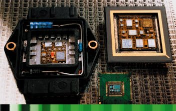
For SoC (system-on-a-chip) prototypes and some low-volume production there is a solution, called MCM-D (multi-chip module-deposition). It allows to combine a controller chip with flash memory as a known-good-die (KGD) on a thinfilm-multilayer-silicon substrate (acting as micro-PCB), and to package this combination like a bigger chip, maybe on a customized leadframe. The Swedish specialist firm Strand is focused on those substrate wafers for MCMs.
Hans-Wolfgang Diesing, businessdevelopment manager, Strand Interconnect
An engineer needs not to be an expert on embedded flash systems-on-chip (SoC) to integrate complex mixed signal, technology and functions into a single IC package. Most embedded microcontrollers and digital signal processors (DSP) are designed to end up as single-chip systems integrating a fair amount of mask ROM firmware for the anticipated mass production. However, the OEM especially in today’s fast pace innovation might not finish off his software development before the volume ramp up is actually taking place and what’s worse: very likely the ultimate revision of the beta version will not be released before the endproduct reaches the peak of lifecycle. Unfortunately, this scenario reflects common business reality. It is not only a problem for the OEM, but also puts the chip supplier into a serious dilemma: the strategically priced (re)programmable version of the system chip (if available) was just intended for SoC prototypes and maybe some low-volume pilot production. It wouldn’t yield well enough in mass production to be even nearly cost compatible with the OEM’s endproduct calculation.
The good news is that there is a solution for this problem – it is called MCM-D (multi-chip module-deposition) type. It allows, for example, to combine the controller core chip with somebody else’s flash memory as a known good die (KGD) on a thinfilm-multilayer-silicon substrate (that acts as some sort of a micro-PCB), and to package this combination like a bigger chip – maybe on a customized leadframe if necessary. At the first glance, this solution might be somewhat more expensive when compared with the embedded mask ROM version, but it usually turns out to be substantially cheaper compared to a bad yielding SoC with embedded flash and still leaving a maximum of flexibility with the OEM.
Si substrates forthinfilm interconnect
Obviously, the most compact multi-chip packages can be achieved with stacked die. Even if the pads are in the wrong place to fit together, maybe there is an option for redistribution of the pads at least on the bigger bottom chip, which should exceed the size of the flash die to some extent. With increasing I/O densities and ongoing structure shrinks, the number of pads mainly defines the chip size, and in some cases there might not be enough room left for thinfilm redistribution and additional interconnect pads. The stacked die approach, however, has some advantages: first, the low thermal expansion and its perfect matching (between silicon and silicon), which avoids mechanical stress over extended temperature cycling and increased temperature ranges as well as the long term reliability of the piggyback combination. The other beneficial property is the high thermal conductivity that is almost comparable to aluminum, which is the most widely used heat distribution material. Last but not least, there are a perfectly polished surface, a standardized form factor and mechanical properties of silicon wafers recommend for thinfilm processing down to 25µm line structures – especially when it comes to spin coating of photolithographic dielectrics on large wafers.
All these benefits apply likewise for the silicon substrate. It is, however, a slightly bigger alternative to stacked die in cases where redistribution of the bottom chip does not work out, or when there are more than two or three chips to be combined. In other words, a silicon based MCM-D is another form of the stacked die approach with an extra level of thinfilm interconnect on a ‘dummy’ chip. Another economical consideration is that separate silicon based interconnect substrates can be processed in a dedicated thinfilm wafer foundry at much lower cost and at less risk of additional yield losses. Silicon can be a low-cost base material when sourced as diffusion reject wafers. Equipment, maintenance and processing costs are substantially lower for thinfilm requirements when compared with the overall cost of a full-blown submicron diffusion fab that provides an expensive overkill in purity and precision for thinfilm deposition and lithography. However, the final assembly and packaging yield of MCMs with silicon substrates from a streamlined thinfilm waferfab is getting close to 100%.
Fresh application ideafor an old technology
The MCM-D approach even incorporating thinfilm-multilayer interconnect on silicon substrates is not at all a new technology. Its development began in the late seventies to follow the growing I/O density demand of mainframe CPUs and later for more compact avionic motherboards in ceramic packages. Both applications were neither volume-driven nor cost-sensitive. That’s why MCMs still seem to have an exotic and exclusive smell. Now there is a low-cost mass production of small thinfilm interconnect substrates on 8-in wafers for multi-chip packaging coming from Strand This company commercialized the previous supercomputer and space age technology for high-volume manufacturing with price tags in the single-dollar range. Not only technical or economical constraints and requirements are driving this development. Also, the pressure from an accelerating innovation rate in highend consumer markets and all the combinations of mobile information technologies is not only demanding improved compactness and performance, but is also asking for fast turnaround in design and production.
With thinfilm layout and processing, innovative chip combinations in a single package can be implemented within weeks instead of months, compared with the design and production cycle of a single-chip-system ASIC. Interestingly enough, the vast majority of inquiries for MCM substrates are coming from the semiconductor industry. Obviously, they have all the internal or external infrastructure respectively to deal with thinfilm layout design as well as with wafer handling, dicing, assembly, packaging and test at competitive cost. In most cases, the backend tasks are outsourced to globally operating subcontractors anyway, and in some instances even designs are done externally.
Strand is focused on production of thinfilm-silicon-substrate wafers for MCM assembly and packaging. For this purpose, a huge production area for processing of8-in wafers was set up. Highly automated equipment allows the entire production line to run with two operators only, so that the impact of labor cost is minimal, also in a country like Sweden. Even qualification and R&D tasks are outsourced to institutes or companies, where the process was developed and the spin-off by Strand was initiated. After the first year in business, a limitation in production capacity is already becoming apparent. So, plans for expansion will be implemented and options for joint ventures in market areas like the US are explored. The foreseeable demand is exceeding the original business plan figures by far.
Look at the basics:thinfilm buildup
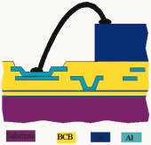
Up to four interconnect metal layers of 1 to 3µm sputtered aluminum can be built up with dielectric interlayers of 3 to 7µm spin-coated polymer called benzo-cyclo-buthene (BCB). It cures within one minute at 250°C, and withstands process temperatures of up to 350°C thereafter. This way it is process-compatible with even lead-free soldering of flip-chips at increased solder temperatures. BCB is photosensitive before curing and can be photolithographically processed without requiring separate resist stripping steps. Another important benefit of BCB is its outstanding low K (dielectric constant) of 2.65 and the extremely low dissipation factor of 0.0008. These electrical properties are the key to desired interconnect performance in terms of signal integrity. Those are low loss, low noise, low crosstalk and interference, which results in higher signal frequency or faster data throughput.
Metal lines are typically 20µm wide with 25µm spacing. Traces can jump over metal layer levels through vias holes in the dielectric interlayer. Bigger top layer vias under an opening in the BCB passivation are used as pads for wirebonds or flip-chip bumps. This way even fine-pitch multilayer PCBs can be outperformed with a fractional number of layers when it comes to multi-chip package versus multi-package assembly. Especially if the excessive I/O density is just limited to a minor part of the board and the rest could get away with a much coarser structure, multi-chip packaging could open up interesting cost saving potentials, since it condenses complex interchip connections into a considerably smaller package pincount with less challenging pitches.
Various assembly methods
There are different assembly methods available for multi-chip modules and packages. The classical approach is wirebond from chip-to-substrate and from the HDI substrate to the bond pads of a ceramic pin-grid array that is either soldered onto a through-hole board or plugged into a PCB socket.
An interesting version is the smart-power substrate on an aluminum plate molded with connector pins and solder posts into a plastic module. It utilizes all kinds of interconnect techniques including through-hole soldering of leaded components, surface mounting of chip components and wire bonding without using any PCB. Thick aluminum bond wires go straight from the top of the discrete power chips to the connector pins even bypassing the substrate interconnect.
Other samples demonstrate the superior compactness of flip-chips on a small silicon substrate on top of a laminate-type ball-grid array. Six flipped chips are mounted next to each other – almost edge to edge – just leaving a bond pad frame on the outer substrate area. The more space consuming wirebonds take care of the connection from the silicon substrate to the epoxy laminate providing a compliant buffer that absorbs the mechanical stress due to the thermal expansion mismatch between both materials. This effect is far from being neglectable as the example may demonstrate. A 10mm silicon substrate expands over 100K by 2.6µm. The same distance from a neutral point on the epoxy laminate will expand by 18µm – that is 15.4µm potential displacement or deformation.
Road map options
How about assembly without packaging? For example, four back-grinded (thinned) flip-chips are surface mounted to a thinfilm-interconnect Si substrate. In addition, since through hole connections cannot be made to the other side of the wafer at reasonable cost, the substrate has big solderballs that exceed the thickness of the thinned chips and thus can be flop-soldered onto the PCB. Obviously, this model would not work with solderballs over larger substrate sizes or extended temperature cycles, but the solderballs could be replaced by more elastic connections like anisotropic conductive adhesives or elastomers, micro springs or stud bumps. If both the substrate and the flip-chips are well passivated, this package-less assembly is likely to withstand even aggressive environments. Other than most organic substances, BCB is extremely moisture resistant and is proven as a superior polymeric IC passivation. In case of doubt, underfilling could take care of an enhanced protection.
Even if all those mentioned challenges are going to be overcome, there is still a sourcing problem foreseeable with external supply of flip-chips. It can be solved by applying stud bumps to the substrate and flip the known-good-die by means of a shrink adhesive, that permanently presses the aluminum ‘bond’-pads of the chip onto the stud bumps and thus gives a reliable connection. This method is already proven at least for smaller volume production, and it does not need any flip-chip redistribution, bumping or underbump metallization. This would require the chips to be supplied in form of a wafer. That is exactly what chipmakers are trying to avoid, because it would disclose most likely their yield performance to their customers or competitors.
Now it seems, that another option will be evaluated by NanoPierce to solve this problem. NanoPierce is plating conductive sandpaper pads on smart card modules and pressglue the back-grinded chip (face down) onto the module surface. The metal-plated microcrystals of the conductive sandpaper pads pierce through the isolating oxide skin of the chip’s aluminum pads, and give a good and reliable contact as long as the adhesive keeps up the pressure on the tips of the conductive microcrystals, that pinpoint-wise alloy with the aluminum pads in some sort of a cold welding process. This technology is currently under evaluation for flip-chip assembly on other substrate base materials than laminates like silicon, for example. As silicon substrates are available in wafer form they can be plated and structured by photolithography in the required 50µm pitch precision.
The advantage over stud bumping would be the replacement of a sequential process with a parallel batch process that obviously would save time and money at least for the flip-chip assembly. Silicon could be the substrate base material of choice, since it should give the best contact reliability over temperature cycling because of its perfect expansion matching with the flipped chips on top. It should avoid erosion of the ‘conductive sandpaper’ pads due to expansion mismatch stresses, and so maintain high contact quality.
EPP 180
Zusammenfassung
Mit Multichip-Modulen auf Silizium-Substrat lassen sich im Halbleiter-Packaging einige wesentliche Vorteile erzielen (beispielsweise keine unterschiedliche Temperaturausdehnung zu den Si-Chips), die den höheren Aufwand für diese Lösung absolut rechtfertigen. Speziell bei der Realisierung von komplexen Systemen in einem Package bzw. auf einem Substrat dürfte diese Technik – insbesondere bei niedrigeren Stückzahlen – mehr Erfolg versprechen als das „klassische“ System-on-a-Chip (SoC).
Résumé
Les modules multi-puces sur substrat de silicium permettent de profiter d’avantages de taille dans le conditionnement des semi-conducteurs (par ex. pas de différence de dilatation thermique par rapport aux puces Si), qui justifient parfaitement le coût supérieur de cette solution. Dans le cas notamment de la réalisation de systèmes complexes dans un boîtier ou sur un substrat, cette technique devrait être plus prometteuse, en particulier avec des quantités réduites, que le „classique“ System-on-a-chip (SoC).
Sommario
Nel packaging di semiconduttori, con moduli multichip su sostrati di silicio è possibile ottenere alcuni vantaggi essenziali (per esempio si evitano le differenze di dilatazione termica tipiche dei chip „Si“) che giustificano senza alcun’ombra di dubbio la maggiore spesa di tale soluzione. Tale tecnica – soprattutto nel caso di quantità ridotte – promette un maggior successo rispetto al sistema „classico“ on-a-chip, soprattutto nella realizzazione di sistemi complessi in un package o su di un sostrato.
Unsere Webinar-Empfehlung
Applikationen aus dem Bereich der Leistungselektronik gewinnen immer mehr an Bedeutung. Die Inspektion dieser Applikation lässt sich mit der bewährten Standardtechnologie der 3D-Messtechnik bewerkstelligen.
Teilen:


