
During wafer-bumping, a high-lead (5/95 Sn/Pb) solder and an RMA flux is used. Because the temperatures reach 340 to 360ºC, flux residues can be polymerized and are difficult to remove. A cleaning agent with high solvency is required, yet must not cause corrosion. The solvent must rinse clean and leave no residue to disturb the die-attach. A semi-aqueous cleaning agent combined with a centrifugal cleaner has rendered to be effective.
Mary Pat McCurdie, Agilent Technologies, Fort Collins, Colorado
Flip-chip packages on ceramic substrates require high-lead solder to be used on the chip due to subsequent reflow processes. The solder is deposited sequentially (lead followed by tin) by an evaporative method. An RMA rosin-based flux is spun over the entire wafer, and the wafer is reflowed in an IR oven under a hydrogenenriched atmosphere. The wafer must becleaned to remove the residue left by the flux. In a rosin-based flux, the most pre-valent compounds are organic acids thatconvert during high-temperature reflow to carboxylic acid. It is important to remove these acid residues because they are hydroscopic, and will contribute to corrosion of the solder. Additionally, during reflow at 340 to 360ºC, the flux is polymerized and the residue can be very difficult to remove. Residue cannot be identified as harmful by visual inspection, therefore it is best to remove all of them. Post-cleaning processes and properties, including die-attach reflow, underfill adhesion, and long-term reliability may be compromised by the presence of these residues.
Wafer cleanliness must meet the following criteria: no active residues that will cause pitting or corrosion during storage may be present; the solder bumps must reflow and wet the contact pads during the subsequent assembly process; the surface must be clean enough to insure good underfill adhesion. It is desirable to have shiny silvery bumps in appearance. The presence of color does not necessarily indicate corrosion products, nor does the absence of color prove the lack of corrosion. Therefore, the ultimate test of wafer-bump cleanliness is the performance of the bumps in subsequent pack-aging processing and use.
Cleaning processselection criteria
In this application, the cleaning system is multiple use. This objective grew from the desire to minimize capital costs, and simplify the manufacturing process. Other requirements include adequately cleaned wafers, the chemistry must be environmentally agreeable, hazardous waste must be minimized, safety of the operators must not be compromised, and the cleaning process (including operation, maintenance and process control) must not be cost-prohibitive.
As part of the low-cost criterion, a triple-purpose cleaning system is desirable. Not only will this equipment clean wafers, but also flip-chip and BGA assemblies. Because the equipment must clean between the die and the substrate in flip-chip manufacturing, in-line aqueous spray cleaners were removed from consideration, as they have no method of delivering the cleaning chemistry to the small gap between the die and substrate. To limit the use of stored Class 1 solvents for safety reasons, vapor-degreasing equipment was eliminated from consideration, too.
A centrifugal cleaner with different fixtures provides the capability of processing several package assembly sizes and both 150 and 200mm wafers. Centrifugal equipment is an excellent choice to deliver the cleaning agent in small gaps and through small channels between solder bumps. Finally, centrifugal processing is compatible with multiple chemistry options, including hydrocarbon, semi-aqueous saponifier and aqueous cleaning agents. The Accel MicroCel is selected for this operation. In this equipment, the wafers are submersed and rotated in the cleaning solution at 80ºC. Following the clean cycle, the wafers are rinsed with DI water at 60ºC and dried with 200ºC air.
The primary requirement for the cleaning chemistry is good flux solvency. It also should be free-rinsing and have a low surface tension and low viscosity so that the fluid will go in to small channels and gaps. Five chemistries were selected for beaker-scale testing on flip-chip assemblies. The chemicals evaluated included semi-aqueous, hydrocarbon, aqueous with saponifier and full-aqueous liquids. Testing eliminated full-aqueous and aqueous with saponifier solutions. Semi-aqueous and hydrocarbon chemicals performed nearly the same in beaker-scale tests. Ionox HC, a semi-aqueous hydrocarbon agent, was selected because it had more desirable characteristics than the other ones. This agent has a high flux solvency, yet very low flammability, a mild odor and is biodegradable.
Results fromanalytical instruments
One of the difficulties in evaluating thecleanliness of wafers is finding an analytical technique. Surface analysis techniques like X-ray spectroscopy for chemical analysis (ESCA) or time-of-flight secondary-ion-mass-spectroscopy (TOF-SIMS) are precise, but are practical only for measur-ing a few sample solder bumps on the wafer. ESCA cannot assign the elemental results to molecules, so it is unknown if the residue is flux or cleaning agent or from another source. Visual techniques, micro-scopic inspection and scanning electron microscope (SEM) are not quantitative, and are also difficult to evaluate over the entire wafer. Gas chromatograph-mass spectroscopy (GC/MS) has the potential to be a valuable tool.
The wafer is rinsed with a known quantity of solvent (here acetone). The solvent is collected and analyzed via gas chromatography. The different fractions then are analyzed with a mass spectrometer. Theoretically, in this manner we can obtain molecular fragment identification and quantitative comparisons of residue. This method was tried with several wafers. Unfortunately, the technique is so sensitive that it identifies molecular fragments from photoresist and the polyimide passivation layer, in addition to flux and cleaning residues.
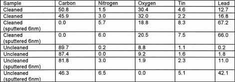
ESCA results (table 1) show that cleaned samples have less or-ganic contamination than un-cleaned samples. All carbon residues are eliminated after a slight sputter on the surface. The uncleaned samples still have a significant amount of carbon present even after a surface sputter.
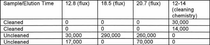
A similar experiment using GC/mass spectroscopy confirms these results (see table 2). The wafers used in this experiment did not have polyimide passivation on the surface. The polyimide tends to complicate the analysis since it provides a source for organic contamination. The molecular fragment eluded at 12 to 4 minutes from the cleaned wafer rinses has been matched with the cleaning chemistry. The amounts displayed in table 2 for the cleaned wafers represent ion abundance measured by the gas chromatograph and translate to sub-microgram levels of contamination. Many fragments eluded from uncleaned wafer rinses match with RMA flux. Types of flux fragments include aliphatic amides, aliphatic carboxylic acids and nonylphenol. For clarity, only two of the fragments abundance levels are shown in table 2. The elution time of 18.5 minutes corresponds to an unsaturated aliphatic acid, and 20.7 minutes to an aliphatic amide.
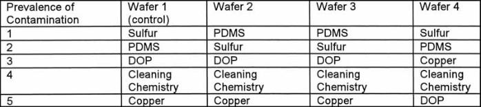
Both ESCA and GC/MS analyses indicate that some of the cleaning agent remains on the solder bumps. This observation is confirmed by TOF-SIMS analysis. Several wafers were evaluated to identify different types of coloration observed on the surface of solder balls. While no conclusions were made regarding color, all of the wafers have residue identified as cleaning chemistry (table 3 for results). By far the most preva-lent contaminants are sulfur, polydimethyl siloxane (PDMS) and dioctylphthalate (DOP). Comparisons with other contaminates found by TOF-SIMS show the cleaning chemistry residue is insignificant. This extremely sensitive tool for surface analysis identifies only the top monolayer of material. Therefore, because tin and lead are the prevalent materials identified, we concluded the contamination will have little effect on the performance of the solder bumps. Additionally, no adverse adhesion or voiding has occurred in the underfill reliability testing of the assembled packages.
Cleaning temperature effects
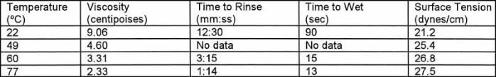
The cleaning agent properties change with temperature. The recommended operating temperatures are 50 to 70ºC, where the optimum solvency, free-rinse properties and surface tension occurs. Data presented in table 4 illustrates temperature effects on the solvent. While surface tension actually increases with temperature, the viscosity and rinse properties are enhanced. Viscosity was measured by a capillary-tube method. Rinse time is the amount of time it takes a dye-doped chemical sample to be removed by DI water from beneath a 2-in die at a 1.5-mil stand-off. Time-to-wet is a similar measurement: a dye-doped droplet has to travel under the length of a 2-in die at a 1.5-mil stand-off. Most of the enhancements to performance occur between room temperature and 60ºC.
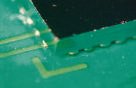
Due to the nature of the evaporative process, small solder balls remain around the bump after reflow. These are referred to as satellites. They are formed during reflow from evaporated solder to a spherical wafer bump. The satellites are not known to be a reliability problem, except for the following hypothesized effects: first, flux residue tends to collect around the base of the satellites, and since this is an active flux, it must be removed entirely to avoid corrosion. Second, satellites form on the passivation layer, and are not adhered as well as the solder bumps to the metalization. Therefore, satellites are a potential underfill failure-mode.
During process development, experiments showed that flux removal was better at 80ºC than at 70ºC. However, at 80ºC the cleaning agent is more aggressive, and causes some degradation in fixtures and seals. An evaluation to compare cleaning at these two temperatures was only partially successful. Because the wafer samples had polyimide passivation on the surface, GC/MS results were not conclusive. Organic other than flux residues dominated the results. SEM has shown that the flux removal is approximately the same for the two temperatures. Initially, the cleaning solvent was changed every 200 cycles. This was calculated to maintain a flux loading level below 1 to 2% by volume. Above this loading, the solvency of the fluid could be compromised. These calculations were worst-case, and based the value on the amount of flux on the parts, not on the amount of flux remaining after reflow. As manufacturing demands increased, the replacement schedule proved to be a bottle-neck. This procedure and subsequent heat-up time was impacting throughput. Additionally, the amount of solvent used and disposed was excessive. Calculations based on estimated flux residue after reflow indicated the cycles prior to solvent replacement could be increased to at least 800. Determining contamination at low levels in the cleaning solvent is difficult. There were no indications that flux is present at the detection limit of around 0.01%.
Control of solution
Due to the centrifugal cleaning equipment design and the elevated process temperature, some of the cleaning solution evaporates during each cycle. When the water level drops, the cleaning capability decreases so, the water content must be carefully controlled. The refractive index is an indication of the amount of water in solution, and is used to indicate when water must be added. As the water level drops, the index increases. To maintain control, a refractometer is used once a week to measure the refractive index of the cleaning agent.
A batch centrifugal cleaning system com-bined with a semi-aqueous alcohol-based agent has been veryeffective in cleaning RMA flux from the surface of wafers in a bumping/flip-chip assembly line. In two years of production, wafer cleanliness has never been identified as the cause of suspect parts or failure. Regularly performed pull strengths from assembled packages show excellent wetting of the wafer bump to the pad. Analytical tests and visual inspections indicate flux residues are adequately removed from the solder bumps. Costs have been minimized by using the centrifugal machine for multiple cleaning processes, and by increasing the time between solvent replacement.
EPP 178
References
K. Dhaneshwar, N. C. Lee: Post Reflow Solder Paste Residue – Sources, Properties, Chemistry and Concerns. Indium Corporation, 34 Robinson Road, Clinton, NY 13323, USA
S.M. Scheifers, C. J. Raleigh: Effects of Flux Contamination on Flip-chip Reliability, Sensors in Electronic Packaging. MED-Vol.3/EEP-Vol. 14, ASME 1995
A. Sinni, M.A. Palmer: Kinetics of Flux Residue Formation in a Humid Environment. IEEE/CPMT International Electronics Manufacturing Technology Symposium 1997
H. H. Manko: Solders and Soldering. McGraw-Hill, New York, 1979
C.P. Wong, W.O. Gillum, R.A. Walters, P.J. Sakach: Reactions of High Lead Solders with BIOACT EC-7R Semi-Aqueous Cleaning Reagent, IEEE 45th Electronic Components and Technology Conference, 1995
Speedline (Accel MicroCel), 1825 East Plano Parkway, Plano, TX 75074
Kyzen Corporation (Ionox HC), 430 Harding Industrial Drive, Nashville, TN 37211
Zusammenfassung
Spezielle Lotperlen definierten Durchmessers stellen den elektrischen und mechanischen Kontakt zwischen Array-Area-Packages (Flip-Chip, BGA) mit den Pads auf dem Substrat bzw. Leiterplatte her. Damit der Reflow-prozeß erfolgreich verläuft, ist Fluxer nötig, der aber die Zuverlässigkeit des Bauteils bzw. der Baugruppe minimieren kann. Für die Reinigung der Wafer nach dem Bumping wurden in einer umfangreichen Studie nun praktisch angelegte Untersuchungen mit differenzierter Analysetechnik untermauert.
Résumé
Des perles de soudure spéciales, d’un diamètre précis, assurent le contact électrique et mécanique entre les Array-Area-Packages (Flip-Chip, BGA) et les Pads sur le substrat ou la carte imprimée. Afin que le processus de reflow se déroule correctement, il est nécessaire d’avoir recours à un fondant qui peut cependant agir au détriment du composant ou de l’ensemble. Pour le nettoyage des tranches de silicium après le Bumping, les analyses pratiques ont été complétées par une technique d’analyse différentiée dans une vaste étude.
Sommario
Delle speciali perle di saldatura a dolce dal diametro definito creano il contatto elettrico e meccanico fra gli Array-Area-Packages (Flip-chip, BGA) ed i Pads sul sostrato o la scheda IC. Per permettere uno svolgimento positivo del processo di reflow è necessario del Fluxer, il quale a sua volta può ridurre l’affidabilità del componente o del gruppo costruttivo. Nell’ambito di un’analisi di ricerca sulla pulizia del Wafer dopo il Bumping, le ricerche a carattere pratico sono state avvalorate con una tecnica di analisi differenziata.
Unsere Webinar-Empfehlung
10.10.22 | 10:00 Uhr | Conformal Coating ist ein wichtiges Verfahren, um elektronische Baugruppen vor dem vorzeitigen Ausfall zu schützen. Damit bekommt der Beschichtungsprozess eine immer höhere Bedeutung. Dabei ist die Auftragsstärke ein wichtiges Qualitätskriterium. Nur eine…
Teilen:


