
The worldwide pressure to move away from traditional lead-containing solders has resulted in some intriguing differences of philosophy and approach around the world. These differences were highlighted during a recent fact-finding mission.
Brian Richards, consultant with the National Physical Laboratory, U.K.
In Europe, interest in using lead-free soldering technologies has been fuelled by proposed legislative restrictions on the use of lead in electronics. These restrictions arose from concerns over lead ending up in landfill and contaminating land and water supplies, and from concerns over lead contamination from recycling operations. The Japanese were quick to note the implications of such environmental legislation in Europe, and, making a virtue out of an anticipated necessity, promoted the commercial and marketing advantages of so-called green electronics, building on their public preferences for green goods and product differentiation. As a result, Japan is now well ahead of Europe and America in developing lead-free soldering technologies.
Three pieces of EU legislation
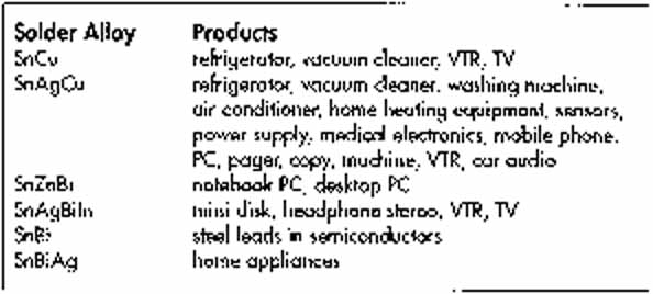
In Europe, Japan and the Pacific Rimcountries there is a general acceptancethat Pb-free soldering will become the norm in the next few years, whether ornot the environmental case is proved. (Figure 1 shows a short list of already introduced green electronics appliances.) However, in America, the debate continues on the financial and overall environmen-tal impact of moving to lead-free technology.
For more than 50 years, lead-containing solders have been used throughout the industry for attaching components to printed circuit boards (PCBs). Such solders are inexpensive, perform reliably, and possess unique characteristics that are well suited for electronics applications. So, in some areas there is reluctance to move away from the traditional (usually SnPb) solders, especially when the evidence for landfill leaching is sparse, and some cradle-grave environmental analyses suggest an overall negative impact of moving to lead-free technology.
Progress of the European legislation has been slow. In 2000, after five years of draft documents and consultation on the original WEEE (Waste from Electrical and Electronic Equipment) proposal, the industry faced three separate pieces of EU legislation:
• WEEE – concerned primarily with minimizing waste and maximizing recycling at end-of-life
• ROHS – concerned with restrictions/ bans on the use of certain hazardous substances (lead)
• EEE – concerned with minimizing overall environmental impact by adopting ”green” design and manufacture, without material bans
It is the ROHS proposal that promises the greatest impact on the electronics manufacturing industry. This was adopted by the commission and is proceeding in parallel with the WEEE proposal. It requires certain substances (including various heavy metals such as Pb, Hg, Cd hexavalent Cr) to be phased out of new equipment by 2006. Although there are some exemptions to this ban on the use of lead (in radiation protection, ceramics etc), soldering is not exempt. The situation is complicated by a separate directive applicable to the automotive industry, the end-of-life-vehicles (EOLV) directive. While containing the same materials bans as ROHS, it does specifically exempt lead in solders for automotive electronics.
There are no such impending material bans in other parts of the world, the emphasis of any legislation being on recycling. However, in Japan impending legislation is no longer the driver. „Corporate environmental consciousness” is the buzz phrase, perhaps a euphemism for winning market share. However, the initiative is top-down driven, and companies do build environmental performance (and rewards) into their corporate plans. Many have published environmental strategies that include eliminating lead in timescales of a few years – well within that of the proposed EU Directive. The JEITA roadmap indicates that full use of lead-free solders in all new products will be achieved in 2003. However, companies in other parts of the world have generally yet to show the same commitment. America, previously disinterested in lead-free soldering, has latterly been spurred into action, although much of its debate centers on the perceived lack of any technological and financial sense in moving to lead-free solders.
The adoption of lead-free soldering will have major implications for the industry. Fortunately, some progress has been achieved in key areas. Although it is widely agreed that there is no drop-inreplacement for SnPb solder, there is a range of possible alternatives commercially available. The trick is to choose the right one for any particular application, and here again there are interesting differences of approach. In general, decisions in Europe and America have been reached on the basis of extrapolation from known materials properties and process issues. In Japan, materials have been ranked in order of suitability based on actual product builds. However, over the past year or so, there has been an increasing consensus for using one family of alloys, based on SnAgCu. This family has the advantages of good reliability and good solderability, but suffers from a slightly higher melting temperature (217OC), and increased cost due to the silver content. Since there are two patented compositions in this family (one American and one Japanese), account must be taken of possible patent and license coverage. Consequently, Japanese assemblers tend to select alloy compositions that fall outside the American patent, i.e. slightly away from the eutectic composition, whereas European and American companies have focused on the eutectic alloy.
The US distinct reluctant
But the choice is still ”horses for courses”, i.e. largely product or application-dependent, when factors such as temperature compatibility or cost respectively may sway the choice. For example, the Japanese have undertaken significant development of SnZnBi (melts at 195°C) for use in ap-plications where there are component temperature issues. In addition, the lower melting point SnAgBi type alloys have been studied for SMT consumer products. While the use of bismuth is widespread in Japan, in America there is a distinct reluctance, on toxicity grounds, to use any Bi-containing solders. The Sn0.7Cu solders are being developed for wave soldering situations where alloy cost is a particular concern, and Matsushita has used them to produce over a million PCBs for its VCRs. The Japanese are much more amenable than their Western counterparts to using silver in wave soldering. They claim the extra cost is minimal but the overall process yield is improved. Interestingly, while in Europe and America the telecommunications industry is in the vanguard of change, in Japan it is the consumer and white goods sectors that are leading the way, probably reflecting the take back targets of its Consumer Electronics Recycling Law.
So the outlook is bright. Performance data, especially those from the field, though sparse, suggest that the Pb-free solders will provide adequate joints. The reliability of SnAgCu, in particular, appears to equal that of SnPb. However, there is a downside – there are still some problem areas in implementing lead-free soldering, and these are viewed differently in different countries.
A major implementation issue is the higher process temperatures required by lead-free soldering. Good temperature control is essential because the processing is much closer to solder’s melting point. Following the European example, Japanese industry now realizes it needs to invest in new reflow oven technology, appropriate for lead-free soldering. Many reflow ovens worldwide are not capable of providing the tight temperature control (small DT) required, and hence capital expenditure for ovens is a big issue.
Some of the processing issues can be eased by nitrogen inerting, which is used widely in Japan. Not only does it widen the process window, but it also allows more flexibility for paste-temperature profile compatibility, e.g. processing SnPb and SnZn solder pastes with the same profile. Other advantages claimed by the Japanese are reduced voiding, particularly with BGAs, and easing of rework/repair operations.
An issue called compatible components
The effects of both higher processing temperatures and longer times raise major concerns over the compatibility of components ranging from plastic encapsulated devices, to capacitors, LEDs, electromechanical components and connectors. Although lower peak process temperatures for lead-free soldering are being addressed through flux and equipment developments and by nitrogen inerting, in many cases the combination of soldering time and temperature for typical lead-free reflow profiles, significantly exceeds that specified on component manufacturers’ datasheets. Published data suggest the incidence of failures is small, which may simply reflect the current low level of Pb-free soldering in the industry. In Europe and America the issue is regarded as essentially one of re-qualification of the components, say to 260°C, a process that is both time-consuming and expensive. But unlike their European and American counterparts, Japanese OEMs have accepted that they must do more to modify the soldering process, rather than expect suppliers to provide parts qualified for higher temperatures. For example, they are looking for alloying elements to lower the solder melting point so that they can stay within 240°C max for reflow soldering. In this way, they not only reduce the need for component requalification and ease component availability worries, but also retain small reflow ovens with a small number of zones.
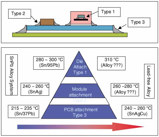
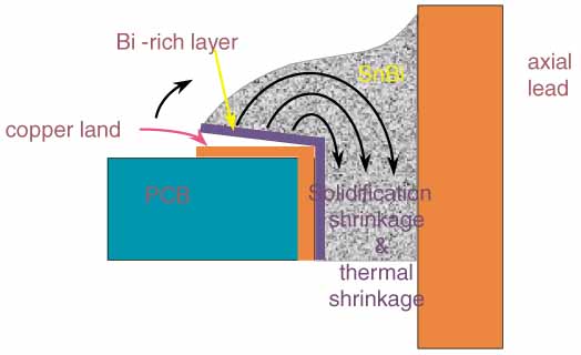
A particular assembly issue is associated with hierarchical soldering (figure 2) in which sub-assemblies are manufactured, using a high-melting point solder that will not reflow during subsequent soldering operations – a technique used without problems for decades. However, in the lead-free era there are issues that have yet to be overcome. While there are lead-free solders suitable for type 3 attachments at low soldering temperatures, there are yet no suitable replacements for type 2 or for type 1. Currently the latter is the high temperature (~300°C) high lead solder, for which no viable alternative has been identified, and any solution is likely to take some time to develop. This situation is well appreciated by the Japanese who are developing alternative systems. For example, silver-loaded resins are being explored to replace type 1 solders, but as with all conducting adhesives, the trick is to make the resin robust while giving adequate thermal and electrical conduction. As for type 2 solder replacement, combinations of the SnAgCu alloy with an underfill resin flux system are gaining popularity.
Component availability with lead-free terminations is perhaps the prime area of concern. In general, component companies have been slow to react to lead-free soldering, possibly due to low customer demand. But this situation is now changing, although in different directions in different countries. A few companies have supplied components with lead-free terminations for several years, but the combinations of lead-free solders and new terminations all struggle to provide the solderability or wire bondability expected from conventional soldering. Similar wetting performance is obtained only when the lead-free soldering temperature exceeds 250°C, i.e. with a similar level of superheat. Each termination material has its own advantages in processing and performance, and a preferred system has yet to be established. In Europe and America, there is a great deal of interest in Pd/Ni. However, in Japan the interest is low, due primarily to cost. Interestingly, in the past two years renewed interest has been shown in developing plating systems for pure tin and tin-based compositions, and in Japan this is now the preferred component finish.
Redesign for higher reliability
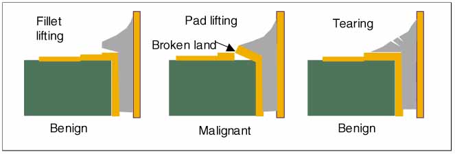
Some performance limitations have been observed when using lead-free solders, the most well-known being that of fillet lifting, particularly in wave soldering and with lead contamination present. Fillet lifting is now recognized as a generic issue for all new solders with PTH components, and even when it is not observed directly, the presence of lead can result in microstructural changes that reduce the strength of the joint with time. Although the phenomenon was first discovered in the UK, the Japanese industry has invested much effort in its understanding, and has now identified three types. Of these, two (”fillet lifting” and ”tearing”) do not cause a reliability issue (i.e. they are „benign”), and only one (”pad lifting”) is malignant. In the latter, peeling ofthe pad from the substrate could destroy the connection, an issue that the Jap-anese are addressing in terms of redesign of pads and resistpattern.
The lack of standards and the wide choice of alloys are seen as limiting progress.But the first steps in this direction areexpected from the Japanese in the nearfuture. It is anticipated that they willrecommend to ISO 9453 two new alloyi.e. Sn3~4Ag0.5~1Cu and Sn3~4Ag2~3Bi.
Whatever the drivers, be they legislation or commercial, and whatever the issues (environmental, cost, awareness, implementation), major electronics manufacturers are already beginning the inevitable transition to ”green” assembly on a global scale. This move, which is already underway in Japan and the UK, is a progressive process starting with the least demanding assemblies. It will accelerate over the next few years, as the perceived barriers to the implementation of the new technology are addressed, and the industry reacts to the combined force of legislation and commercial benefits.
EPP 187
Zusammenfassung
In puncto Übergang zur bleifreien Fertigung ist das weltweite Szenario sehr unterschiedlich. Nicht nur, daß man in Asien, Europa und USA unterschiedliche Lotlegierungen favorisiert, auch die Einstellung zum Thema ist höchst unterschiedlich: In Europa sieht die Gesetzgebung eine Verbannung von Blei spätestens ab 2006 vor, in Japan soll ab 2003 grüne Elektronik dominieren und in USA wird vermutlich eine auf Linie des Anti-Green-Fighters Bush getrimmte Administration zusammen mit Lobbyisten finessenreich die Verzögerung auf die Spitze treiben.
Résumé
Des scénarios très différents se déroulent de par le monde en ce qui concerne le passage à une fabrication sans plomb. Non seulement on favorise des alliages différents en Asie, en Europe et aux USA, mais les opinions divergent également très fortement sur le sujet: En Europe, la législation prévoit un bannissement du plomb en 2006 au plus tard, au Japon, l’électronique “verte” devra dominer à partir de 2003 et aux USA, l’administration de l’anti-écologiste Bush et les lobbies ne vont probablement pas manquer de repousser l’échéance à l’extrême.
Sommario
Per quanto riguarda il passaggio alla produzione senza uso di piombo, lo scenario mondiale è molto differenziato. Non solo per il fatto che in Asia, in Europa e negli USA si favorizzano differenti leghe per la brasatura, ma anche perché questo tema viene considerato in maniera differente: in Europa la legislazione prevede l’abolizione del piombo al più presto a partire dal 2006, in Giappone l’elettronica “ecologica” deve essere sul mercato già dal 2003 mentre negli USA l’amministrazione Bush, fedele alla fama di “Anti-Green Fighter” del presidente, riuscirà insieme ai lobbisti a ritardare quanto possibile l’entrata in vigore di tali normative.
Unsere Webinar-Empfehlung
Applikationen aus dem Bereich der Leistungselektronik gewinnen immer mehr an Bedeutung. Die Inspektion dieser Applikation lässt sich mit der bewährten Standardtechnologie der 3D-Messtechnik bewerkstelligen.
Teilen:


