Part I of this article series (published in EPP Europe 9/10) introduced microelectronic grade silicones, which have a combination of properties making them well suited to IC packaging. These characteristics include flexibility/stress relief, thermal stability, moisture resistance, excellent electrical properties, low ionic impurity levels and alpha particle emission. Silicone also offers good compatibility with board substrates and processing techniques, and can bring significant advancements in device reliability and longevity for both wire and lead-bonded designs.
By improving performance and reducing failures of the integrated circuit package, silicone materials help satisfy the demand for smaller, lighter and more reliable components. Microelectronic grade silicones are currently being used in the commercial production of flash, SRAM and DRAM devices, as well as CPUs and ASICs. These low-outgassing formulations deliver JEDEC Level I moisture resistance and proven thermal cycling reliability, while protecting the die from alpha particle emissions released by solder. (Ann Norris and Udo Pernisz: Low Alpha Particle Emitting Silicone Materials for Microelectronics.) Silicones can generally be designed into a reworkable package requiring no underfill.
Wire-bonded packages
Wire bond packages are by far the most common designs in the industry. Basedon the generations of epoxy-overmolded chips, which preceded the development of the CSP, the wire-bonded chip scale package makes use of an existing infrastructure of equipment and processing methods. Manufacturing personnel already familiar with overmolded devices typically find little difficulty in this technique.
The first chip scale components to appear on the commercial market were flash memory devices, where the small size and perimeter bonding of the chip means that physical and thermal stresses are shared fairly equally across the entire package. One reason silicone performs well in these applications is its ability to accommodate the mismatched coefficient of thermal expansion (CTE) between the die and substrate.
As the silicon die size and operating temperatures of CSPs have increased with greater density and higher performance, manufacturers are faced with larger components that have non-uniform stresses during thermal cycling. While the center section of the chip may move primarily along the Z-axis when temperatures rise, the corners may exhibit a twisting motion. In addition, with a larger die such as the newest DRAM designs, the components are center-bonded, severely restricting the X and Y-axis motion of the silicone die attach or encapsulant.
All these factors complicate the stresses in a package, and add to the demands made on packaging materials. When first-gen-eration materials showed that the cur-rent silicone formulations permitted toomuch thermal movement and transferred stress to the leads, Dow Corning developed materials having a similar modulus, but with a lower coefficient of thermal expansion. The reduced thermal movement helps protect the die and leads from damage caused by mismatched CTE between the component and the board in large wire-bonded CSP designs. This ability to customize the level of CTE, while retaining compliancy needed for new designs is viewed as an important feature of silicone materials.
Film adhesives and encapsulants
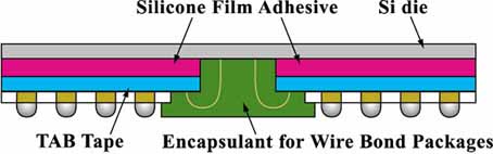
As shown in figure 1, silicone film adhesives for wire bond applications are supplied as a pre-cured film that creates a uniform layer of stress relief. The materials have demonstrated excellent adhesion to both the silicon chip and TAB tape substrates. Compatible with automated punch-in-place equipment to achieve the desired shape, their adhesion is activated with temperature and pressure. Cover films release under light peeling force for easeof operation and high throughput. These silicone film adhesives were developed with stable physical properties for robust wire bondability over a wide range of processing conditions, including:
• Thermal compression ball bonding with heat
• Thermosonic ball or wedge bonding pressure with heat (150 to 250°C)
• Ultrasonic wedge bonding pressure with vibration (60 to 120kHz)
Microelectronic grade silicone adhesives used as the stand-off are specially formulated, low migration materials designed for effective use in wire bonding. The final step is encapsulation of the leads. Silicone encapsulants are used for wire bonding, and can be either dispensed or stencil-printed to meet individual application requirements. These one-part, addition-cure formulations provide mechanical and environmental protection for wire bonds. The elastomeric nature of the cured coating provides excellent adhesion and stress relief to complement the action of thefilm adhesive. Microelectronic grade silicone encapsulants used as the stand-off are designed specifically as low migration materials for effective use in solder reflow.
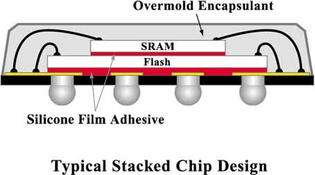
Stacked-chip designs have also provided an opportunity for silicone materials (see figure 2). Used as an elastomeric, shock-absorbing adhesive film on top of the board and in between the stacked die, silicone materials can relieve the stress of thermal movement between dissimilar substrates, helping to prevent device fatigue, solder ball cracking or wire lead breakage.
Lead bond packages
The enhanced reliability of leaded-bond CSPs has been demonstrated in the µBGA package (developed by Tessera). Engineers have worked with materials and equipment suppliers to create an extensive infrastructure to support the lead-bonded design. Believed to offer the highest reliability of any CSP currently available, silicone materials are a key to the µBGA design, relieving the stress on solder balls, yet delivering the right amount of flexibility to protect leads from movement caused by thermal cycling.
Unlike rigid epoxies, which transfer thermal stress to the solder balls, low-modulus silicones for lead bond applications absorb the movement from the mismatch of CTEs. Further, the hydrophobic nature and gas permeability of silicone permits low levels of trapped moisture to escape at elevated temperatures, while epoxies can have a tendency to popcorn from trapped water vapor as temperatures rise. The shock-absorbing capability of silicone elastomers also lends durability to CSPs. When an electronic device is accidentally dropped, the compliant layers of silicone can help protect components from damage across a very wide temperature range, in contrast to alternative materials which experience a significant modulus rise at low temperatures.
Encapsulants, spacers and adhesives
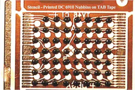
Figure 3 illustrates silicone nubbins on TAB tape for a µBGA package, where silicone materials have been proven as a protective encapsulant, compliant spacer and die attach adhesive. The silicone spacers (nubbins) can be either dispensed or screen-printed, and specific material formulations are available for either technique. In alternate µBGA designs using film adhesives (also known as pad designs), the key differences are the ap-plication method and equipment, as well as the form of the silicone material. The excellent reliability of both package designs requires effective adhesion to the tape and die, co-planarity and stress relief ability.
One of three methods is generally employed to encapsulate µBGA packages: dispensing under ambient atmosphere and curing in an autoclave, vacuum dispensing or vacuum injection. The latter technique enhances material flow and helps reduce process time, contributing to higher reliability and lower cost. Vacuum injection also facilitates the development of more advanced package designs, allowing increased die packing density and the ability to encapsulate a broader range of devices, such as fan-in/fan-out packages. This approach can be used to simplify processing, since complex dispense patterns are not required.
For both the nubbin and pad processes, the company supplies compliant adhesives which compensate for CTE mismatch between die and substrate, significantly reducing the stress on solder balls during thermally caused movement. In addition, microelectronic grade silicone encapsulants help increase the life of the solder joint, without the need for underfill, delivering both processing advantages and performance benefits.
CPU manufacturing
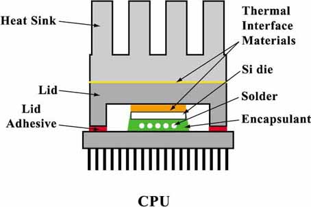
Most conventional CPU designs have an underfilled flip-chip on the substrate, usually with a thermally conductive lid and then a heat sink on top, as shown in figure 4. Because a thermal compound is needed as an interface between the back of the chip and the lid, silicone is used to absorb the mismatched CTEs of the differentmaterials and provide as little thermalimpedance as possible. If a rigid materi-al is used, there can be too much movement between substrate and lid, causing the seal to break or warp the board. Gel materials tend to work better than ther-mal greases, as their greater stability avoids a condition known as ”pump-out,” in which the polymer can separate from the filler.
CPU manufacturers generally put the lid on the device, allowing individual computer OEMs to install the heat sink according to their own specifications. When an adhesive is needed to attach the lid to the substrate, a silicone material acts as a very effective sealant, because of the high elongation and ability to maintain excellent strength through a cross-linked formulation. Silicone materials for these applications can be either electrically conductive (to avoid the need for EMI shielding by grounding the chip to the lid) or electrically insulating. Thermally and electrical-ly conductive silicone materials are also used as a lid seal, die attach or thermal interface material between the lid and heat sink.
Wafer level technology
An emerging technology in the IC packaging industry is wafer level (WL) packaging, where the packaging operation is performed directly on the wafer, rather than packaging after the die are singulated. Although there are many types of emerging wafer level designs, a majority of wafer level packages utilize a redistribution concept to move the signals from a peripheral layout to an area array.
A key to wafer level redistribution technology, just like other package types, is the reliability of the final package in the application. Just as silicone is the material of choice for high-reliability uBGA packages, Dow Corning is also developing silicon-based materials for WL package designs. Silicone materials for use as stress buffer layers can be formulated to achieve a wide range of hardness levels, including the lowest possible modulus of any material used in device packaging. For wafer level packaging manufacturers using a parallel approach (typically a packaging foundry) or series approach (associated with frontend IC manufacturing), the supplier can leverage its technology in spin-on, low-k dielectric materials or encapsulant and die attach elastomers to provide silicon-based chemistry solutions to wafer level packaging designs.
Outlook
Silicon-based materials are currently used in a variety of applications for high volume semiconductor packaging operations. As manufacturers seek to satisfy industry needs for smaller, lighter and more reliable components, low-volatility, high-purity microelectronic grade silicone formulations help improve performance and reduce failures of integrated circuit packages.
Industry trends continue toward greater use of CSP designs with higher transistor density, driving up service temperatures and increasing thermal stress. The ther-mal stresses are even more pronouncedin CSPs in comparison to SOPs/TSOPs. These conditions reinforce the rising use of silicon-based materials for die attach, spacers and encapsulation. Dow Corning has been a world leader in silicon-based technology since the company’s inception in 1943. Its technology can be found throughout the electronics manufacturing process: hyper-pure silicon for wafers, low-k dielectrics for semiconductors, microelectronics grade adhesives, encap-sulants and coatings forIC packaging, and board-level adhesives, conformal coatings and encapsulants.
EPP 188
Zusammenfassung
Zum Vergießen von Hableiter-Packages kann man Polymere oder Material auf Silikonbasis verwenden, wobei sich letzteres nach dem Aushärten durch eine hohe Flexibilität auszeichnet. Silikone bieten viele Vorteile. Neben dem Schutz gegenüber Umwelteinflüssen puffert beispielsweise das Material auch den mechanischen Streß ab, der durch die unterschiedlichen thermischen Ausdehnungskoeffizienten der verschiedenen Materialien von Chip und Laminat auftreten.
Résumé
Pour le moulage des boîtiers de semi-conducteurs, on a utilisé des polymères ou des matières à base de silicone, ces dernières se caractérisant par leur grande flexibilité après le durcissement. Les avantages des silicones sont nombreux. Outre la protection contre les influences de l’environnement, ces matières absorbent également par exemple le stress mécanique dû aux différences de coefficient de dilatation thermique des matériaux du chip et du stratifié.
Sommario
Per la fusione di packages di semiconduttori é possibile utilizzare polimeri o materiale su base siliconica, materiali questi ultimi caratterizzati da un’alta flessibilità dopo l’indurimento. I siliconi offrono molti vantaggi. Oltre alla protezione dagli agenti atmosferici il materiale funge anche come tampone contro lo stress meccanico, generato a causa dei differenti coefficienti di dilatazione termica tipici dei chip e dei laminati.
Unsere Webinar-Empfehlung
.png)
Die 3D-Messung und Inspektion des Lotpastendrucks ist ein wichtiges Qualitätswerkzeug. Dieses funktioniert nur mit den richtigen Toleranzen und Eingriffsgrenzen.
Teilen:


