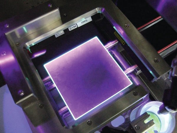
Driven by high pricing and manufacturing costs pressure in the photovoltaic industry worldwide on the one, the need for new and innovative manufacturing solutions for photovoltaic module manufacturing on the other: for the application of mounting and contacting junction boxes onto photovoltaic modules Schiller Automation identified a high potential making this process easier, much more reliable and above everything much more cost effective compared to what the industry is used to. As the junction box itself is one of the photovoltaic inhibited components, that if they do not reliably work, they can become cause of severe quality problems relevant for module failing and eventually fall outs. As photovoltaic module makers do have a sensibility for this issue, the surface mounting, contacting and isolation is designed multi process. This makes the junction box application process relatively slow, failure sensitive and often requires multiple line workers as the process is often conducted manually in order and attempt to achieve the required quality level.
The companies application combines all surface mounting and contacting processing steps in one process and is completely on the fly. So not only much less material is being involved but also and in due course cycle times of 20 s per e.g. 60 cell crystalline modules or thin film technology modules in any GEN5 format can easily being achieved. Another advantage is that the cycle time is scalable, so it effectively can adapt scaling effects during product life time and there-fore ideally fits in multi MW factories. Also the reduced net footprint of 30 m2 combined with best of class logistics of material flow secures best Capex and Opex.
The modular concept of the process also allows an easy integration into existing lines where a cost optimization on CoOModul level gets of competitive relevance. Furthermore this fully automated SMT junction box application inhibits the preparation of the contacting PINs (ribbons) for interconnection with the junction box contacts itself. No manual intervention is required. The contacting PINs (ribbons) will have no de-orientation pre or post laminating. On surface mount level no preparation like surface treatment is required. Together with Henkel a special adhesive system for this application has been developed. The concept of a one step SMT including electrical contacting was developed based on Phoenix Contact junction box technologies. Both Henkel and Phoenix Contact are strategic processing partners to us. Based on this longterm oriented partnership we take over the process responsibility; this secures not only the value of our customer capital investment over time but also enables a managerial dynamic cost control on all operational expenditure. Another photovoltaic industry relevant issue: our processing concept is covering that the contacting technology itself already today is designed to be fully compliant with the upcoming RoHS regime for photovoltaic products. On the manufacturing and application processing level we strictly pursued a so called no waste and green manufacturing approach.
Unsere Webinar-Empfehlung
10.10.22 | 10:00 Uhr | Conformal Coating ist ein wichtiges Verfahren, um elektronische Baugruppen vor dem vorzeitigen Ausfall zu schützen. Damit bekommt der Beschichtungsprozess eine immer höhere Bedeutung. Dabei ist die Auftragsstärke ein wichtiges Qualitätskriterium. Nur eine…
Teilen:


