

For some time, the configuration limitations of photovoltaic metallization lines have cast a long shadow over production possibilities. In today’s fast paced industry, solar cell manufacturers are targeting two key areas: enhanced cell efficiency for more power per square meter of surface area, and increased productivity from the manufacturing process. However, as economic, industrial and political goalposts move around them, manufacturers are faced with the potential cost impact of what they need today not being necessarily what they will need tomorrow.
Darren Brown, DEK Solar, Weymouth (England)
Equipment investment becomes paramount to a cost-effective business model and until now, the necessary flexibility, configurability, modularity and scalability simply did not exist to deliver the required level of value. The recent introduction of DEK’s enhanced Eclipse metallization line has the potential to redefine what manufacturers can expect from their PV production line thanks to an innovative, entirely flexible design concept.
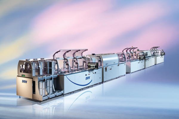
Eclipse is a very high throughput complete metallization solution for commercial solar cell production. Deploying patented multiple print heads operating in parallel, if one head halts for operator attention, the others continue to print to virtually eliminate downtime. Delivering six-sigma repeatability at class-leading accuracies, Eclipse reaches print speeds of 600 mm/sec while also minimising breaka- ges through advanced handling technology. Customer data feedback evidences this at less than the industry standard 0.2 %. However, Eclipse’s real advantage comes in the form of its highly flexible design concept that incorporates a series of field retrofittable process modules that enable manufacturers to scale production up or down as demand changes.
Eclipse today and tomorrow
In fact, the only decision solar manufacturers need to make up front is which way the line runs – from left to right, or from right to left. From this point onwards, it is only necessary for line users to purchase what they need today, without compromising possible requirements for tomorrow. Key Eclipse process expansion modules including the print head and unloader, are designated with a master unit; lead modules that feature master controls. Every second and subsequent process module functions as a slave unit. By not repeating the control modules, true scalability is also considerably more cost-effective.
A scalable advantage
Today, productivity drivers from the most progressive manufacturers are calling for throughputs in excess of 1200 wafers per hour from each metallization line. However, given the fast-paced nature of today’s solar manufacturing environment, it is certainly feasible that manufacturers may need to increase throughput even further in the future. Eclipse is available with true throughput of 1200, 2400 and 3600 wafers per hour thanks to its multiple, simultaneously functioning, print heads. And, since the platform is completely configurable, it is possible to add in an extra printer module to scale up throughput for example. Inevitably, this will have an implication on line formation, knocking existing set up out of synchronisation. However, manufacturers targeting throughput increases in future do not have to go to the unnecessary lengths of investing in an additional printer before they are ready to accommodate it. Instead, the flexibility of the Eclipse line means that DEK can install blank process modules. Simply consisting of an extra length of conveyor, these units can easily be replaced with an extra printer when demand dictates such a move. A future-proof strategy, this unique set-up delivers the flexibility that is now demanded by the most progressive PV manufacturers.
Future-proof productivity
Along with a future-proof design, Eclipse is also equipped to deliver the efficiency improvements required to drive down the all important cost-per-watt metric into the future. For example, one obvious route to increased cell efficiencies is to reduce the size of energy collecting features so they do not shadow underlying silicon substrate. The solution is to give finer lines more height, printing the lines twice over in a print-on-print process that effectively doubles grid height and current-carrying capacity. Known as Print-on-Print, this technique is enabled by repeatable accuracy. Alignment must be perfect, particularly true for the second pass where the landing area – formed by the first print – is so limited that a misalignment of even 10 µm can result in printing paste flooding out and ruining not only the print but the entire cell. With demanding processes such as print-on-print fast becoming standard practice, Eclipse delivers six-sigma print-on-print capability (PoP) ±12.5 microns at 2 Cpk.
Increasing production
It is impossible to predict exactly what the future holds, although we know with efficiency improvements such as print-on-print emerging, grid parity cannot be too far away. Future-proof production is therefore essential, but it must be balanced against value and cost-of-ownership. Paying for what you need today, should not cost you more tomorrow.
Flexibility then becomes one of the most sought after commodities in today’s industry, a stepping stone into a future of higher productivity, throughput and yield. Eclipse embodies this concept through its highly flexible modular design. And, as more and more equipment manufacturers follow suit, increasing production possibilities are moving into the light.
Unsere Webinar-Empfehlung
.png)
Auch dieses Jahr präsentiert Koh Young wieder aktuelle Trends und „State of the Art“ Technologie aus der optischen Inspektion und 3D-Messung auf der Productronica in München. Aber wir alle kennen das Problem voller Terminkalender, Reisebeschränkungen oder fehlender Zeit, um in…
Teilen:


