
The electronic manufacturing service provider Plexus‘ production model can be described as high mix. This means frequent changeovers and relatively small single lots, but in higher numbers. The entire volume is nonetheless high, and extremely varied: it ranges from single-sided, through-hole to complex double-sided reflow assemblies with BGAs requiring selective wave soldering.
Tim Pitsch, Mike Yuen, Plexus Electronic Assembly Corp., Neenah, Wisconsin
Virtually every conceivable type of board assembly challenge is encountered at the EMS company at one time or another. While wave soldering assemblies, bridging in specific and definable areas on them – such as on connectors – is a frequent and predictable problem. Such bridging cannot easily be remedied, and results in rework and slowdown of production for that run or that product exhibiting the problem. We do not design all of the products we build. Many times we rely on our customers and their designs, and they don’t necessarily conform to the way that we set up our equipment. From the EMS provider standpoint, redesigning a PCB is not always an option. Many times, the EMS provider is at the mercy of the customers and the PCB designers to conform to the design for excellence (DfX) preferences.
Recurring bridging problems on high-density multi-pin connectors prompted Plexus to investigate debridging technology. It was realized that there are two contributors to these defects, mainly poor board design and use of a selective wave pallet. Here we will focus on the process-related issues, and the yield improvement gained with a selective debridging device.
Solder bridge
A solder bridge is usually caused by an unstable transitional mode, which occurs in the peel back region of a solder wave. A critical peel back situation occurs when the solder meniscus has to retract abruptly from the board to the wave. The amount of molten solder in the peel back region will ultimately determine the formation of a solder bridge. With subtle disturbances of solder at the molten stage, the wetting equilibrium of solder can easily be shifted. Therefore, it is important to realize that the formation of solder bridges can be related to both the assembly and the soldering process.
Finding and repairing solder bridges after wave soldering can be costly and labor intensive. In addition, it is commonly believed that repaired solder joints are less reliable during the life of the device. Over the years, many techniques have beendeveloped to reduce solder bridging during the final stage of the wave soldering process.
Selective debridging
Selective debridging using air-knife technology has been a standard technique used in wave soldering, but the application tends to disturb good solder joints indiscriminately as well as problem areas. Increased sophistication in process control and computer control, and an integral board tracking system have enabled the practical development of a selective debridging tool for integration into the wave soldering process. The selective debridging technology allows selection of defect prone areas to de-bridge, and leave all the other „good“ solder connections on the board untouched.
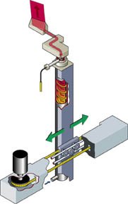
Selective debridging is achieved by applying a tuned gas flow selectively and narrowly to a specific area where solder bridging may occur (figure 1). This is possible because the tool performs its debridging while the solder is still in molten form, immediately after the assembly exits the last solder wave (figure 2). Area dimensions and other process parameters are programmed and controlled by computer. The ability to tune the gas flow specifically, and bring the nozzles into very close proximity to the PCB without contact, is key to the effectiveness of selectivity debridging.
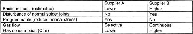
Prior to making a decision regarding the selective debridging system, we compared conventional air-knife with a selective debridging technology. Table 1 compares the air-knife technology between these two vendors. It should be noted that supplier B’s air knife technology was not considered for further investigation due to a number of reasons including incompatibility with existing equipment and overall cost effectiveness.
In an attempt to quantify the effectiveness of the selective debridging system, we selected six sample assemblies for the evaluation studies. The selection of these boards is based on historic production data with known design related solder bridge defects. These assemblies include different component packages, such as flat chip, SOIC, DIP, SOT and high I/O multi-pin connectors.
As shown in table 2, the defect level of these production assemblies reduced significantly using the selective debridging system. However, the small sample size of these tests could not statistically conclude the effectiveness of the debridging tool. Therefore, a larger scale in-house evaluation was performed.
The selective debridging system was evaluated for three months before it wasapproved to be installed permanently. With approval from our customers, the vendor installed the selective debridging system in one of the wave solderingmachines. Data, such as yield, downtime, operating costs and maintenance, was included in a comprehensive evaluation. This trial involved eight different, high-complexity assemblies. The average defect per unit (DPU) improvement was found to be approximately 84%. The team discovered that the selective debridging system was not really plug&play for the user. The degree of success of the selective debridging system depends mainly on board design, optimization of process parameters, and tooling design.
Spray pattern
Since the debridging tool disrupts the equilibrium of the solder bridges selectively, there was concern with the control and definition of the spray pattern. A special test pallet was used to study the spray pattern of the nozzle. A piece of thermally sensitive paper was sandwiched between the pallet cover and a patterned PCB. The idea of this design was to detect thermal changes experienced by the surface of the PCB. With all the heating elements deactivated, the only pattern recorded on the thermal paper was created directly by the debridging device.
By reviewing these thermal images recorded on the paper, it was easy to determine the difference between the pro-gramming parameters and the actual spraying areas. The major findings are as follows:
• The width dimension is consistent with the programmed parameters
• The spray pattern revealed non-uniform thermal exposure at the boundaries
• Excellent length control at low conveyor speed
• Excellent pattern definition at low conveyor speed
To improve the nozzle spray pattern, another zone was added. Its main function was to redirect nozzle to areas of the PCB where the joints would not be disturbed. So, the definition of the test patterns became more stable and legible.
Influence of temperature
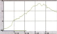
As documented in the company’s internal wave operating guidelines, all solder side components are restricted from exposure to temperatures higher than 270¡C or thermal spikes greater than 4K/sec. To confirm these restrictions were not violated using the debridging system, the thermal profiles of a sample assembly were examined. Figures 3 and 4 show that the thermal stress experienced by the wave side components is relatively mild. Most importantly, the debridging device did not violate any thermal restrictions specified in the company’s internal wave soldering guidelines.
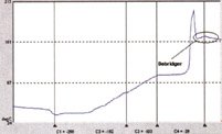
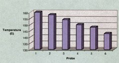
However, the thermal paper study indicated that there are some concerns with the uniformity of thermal exposure. To better understand the thermal charac-teristics of the debridging device, six thermal probes were attached to a samplePCB. The objective of this exercise wasto determine the temperature differ-ence across the debridging tool’s programmed spray areas. To simulate the thermal impact of de-bridging, a 3 x 3-in spray pattern was programmed. It is important to remember that excess temperature gradients across the spray pattern can potentially generate local warpage within the spray areas. Figure 5 indicates that the temperature difference across the spray area is within 6K. This, in turn, should have minimal impact on the overall stress experienced by the substrate and the components. Also, this confirms the temperature at the edge boundaries is slightly higher.
Production Data
The ultimate test of the debridging system’s ability to reduce solder bridging is its effectiveness in a real productionenvironment. It was anticipated that the debridging system could be used to accurately remove solder bridges from wave soldered assembly. In some cases, it has been reported that this technology could even remove solder balls on the component solder side. Since solder balls format random locations,it was concludedthat the quantitative measurements of solder balls on the boards are not practical for the trial.
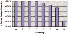
Compared with the original process, the selective debridging system has shown consistent improvement in reducing solder bridges. Figure 6 summarizes the results of the defect data since the installation of the selective debridging system. It should be noted that the solder bridgewas completely eli-minated on assemblies A and B, whereno wave pallet was used.
Cost analysis
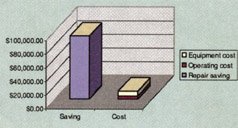
Figure 7 illustrates the cost savings a-chieved by the selective debridging system on a wave-soldering machine. It is important to remember that the level of solder bridge reduction depends highly on component layout, component mix, wave pallet style, and wave soldering equipment. Depending on the variation of these variables, the estimated repair savings could be different. The cost scenario is determined by the following topics:
• Equipment cost assumed five years depreciation plus spare part cost
• Repair savings based on the estimated cost for inspecting and removing a solder bridge.
• Operation cost including gas consumption, electrical power, setup and maintenance.
Compared with historic defect data, the team found that the proper use of theselective debridging system could successfully reduce the number of bridges. This, in turn, improves Plexus‘ ability to effectively process assemblies with undesirable wave design features. The evaluationresults also show that the ability of thedebridging system depends highly onthe assembly design and pallet style.Assemblies processed in selective wave pallets proved to be more challengingthan assemblies that ride directly on fingers or in adjustable pallets. This was partly caused by the limited openingof selective wave pallets. Furthermore,the debridging system was found towork especially well in removing solder bridges on multi-pin, trough-hole com-ponents.
Fax +31-162-483-253
EPP 171
Zusammenfassung
Gefürchteter Effekt beim maschinellen Löten von Baugruppen ist die Brückenbildung durch Zinn, insbesondere bei Wellenlötverfahren häufiger zu beobachten. Untersuchungen bei einem Dienstleister der Elektronikfertigung ergaben, daß man mit einem selektiven Debridging-Tool, eine Art Air-Knife (Luftmesser) die Brückenbildung drastisch reduzieren konnte. Damit steigt in der Fertigung die Ausbeute (First-Pass-Yield) beträchtlich, wobei die Aufwendungen für Reparatur/Rework deutlich zurückgehen.
Résumé
La formation de ponts par l’étain lors du brasage automatique de cartes est un effet redouté, que l’on rencontre plus particulièrement lors du brasage à la vague. Des études faites dans la fabrication électronique ont montré qu’un „debridging-tool“ sélectif, sorte de „air-knife“ (couteau à air), permettait de réduire considérablement la formation de ponts. La production y gagne énormément en rendement (first-pass-yield) et les réparations/retouches sont fortement réduites.
Sommario
Un effetto temutissimo durante la brasatura automatica di gruppi costruttivi è la formazione di ponticelli da parte dello stagno, effetto che si presenta con particolare frequenza nel caso del processo di brasatura ondulata. Delle ricerche effettuate presso uno stabilimento per componenti elettronici hanno mostrato che tramite un Debridging-Tool selettivo, una specie di Air-Knife (coltello d’aria), sarebbe possibile ridurre notevolmente la formazione di tali ponticelli, permettendo di aumentare il rendimento della produzione (First-Pass-Yeld) e di diminuire gli oneri per la riparazione o il reworking.
Unsere Webinar-Empfehlung
.png)
Auch dieses Jahr präsentiert Koh Young wieder aktuelle Trends und „State of the Art“ Technologie aus der optischen Inspektion und 3D-Messung auf der Productronica in München. Aber wir alle kennen das Problem voller Terminkalender, Reisebeschränkungen oder fehlender Zeit, um in…
Teilen:


