


Vertical-contact probe cards for the wafer test offer multiple advantages as it allows for full array test, and high flexibility in parallel probing. Several dice can be probed and tested simultaneously, regardless of the pads’ arrangement. Parallel test strategies can remarkably reduce the cost situation.
Klaus Giringer, Manager Micro Adaptation, Feinmetall, Germany
Epoxy rings are still the most widely used test methodology for wafers. The ring assembly consists of probe needles, horizontally set and firmly embedded into a hardened epoxy ring, according to the cantilever principle. While contacting, the needles bend until the desired contact force is achieved. The pace of innovation in semiconductor technology and the continuous efforts for cost saving creates requirements for probing, which epoxy rings can no longer fulfil.
Full array probing
The growing usage of flip-chips and other array bumping techniques require the contact of numerous of pads on one square centimeter. This application can not be performed with epoxy ring probe cards because there are many physical limitations caused by the horizontal arrangement of the needles.
An increasing throughput of a probing line leads to a reduction of test costs, and as a consequence, also in a reduction of the production costs. Therefore, the objective is to test as many chips as possible simultaneously, minimizing the number of touch downs per wafer. Epoxy ring probe cards require that the pads on the wafer are arranged in certain patterns, using parallel probing, again caused by the physical limitations in the horizontal arrangement of the needles. Often the parallel probing with epoxy ring probe cards needs to already be considered in the chip design. This represents a few limitations in the application of parallel probing.
High temperature range
The temperature range during the die test expands more and more. For several types of probing methods, temperatures between 0 and +125°C are required. The conventional probing card technology clearly shows its limitations here, too. The structure of a needle card is extremely complicated and difficult to control, in respect of the thermal behavior.
Vertical-contact probe cards provide an answer to higher probing requirements. The principle on which a vertical probe card is based on is the buckling-beam (or buckling wire). Mathematical equations define the bending or buckling of columns as a function of loads placed on them. This relationship show that, if a force take effect on the end of a wire, the wire will bend and generate a spring force that is almost independent of the amount of the wire’s displacement. The graph of the force is generated as a function of displacement for a buckling wire and, as a comparison, for a compression spring. In contrast to the spring principle of a needle card, a strong non-linear spring characteristic is achieved, resulting in homogenous distribution of force over all contacts of a vertical probe card.
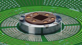
For the past eight years, Feinmetall has applied buckling beam technology to test substrates in the fine-pitch range, where the probing pads are contacted in an array grid of about 200µm. Since wafer probing requires the addressing of considerably higher contact densities and smaller contact surfaces, we have developed this technology to meet the requirements of wafer probing. The result of this effort is the ViProbe (Vertical integrated Probe Card). The decisive innovation is a method to drill finest holes into the guide plates and the application of adequate contact materials.
Characteristics of ViProbe
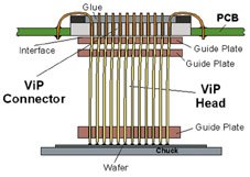
The vertical probing assembly consists of the ViP head, which contacts the wafer (DUT) and the ViP connector, ensuring a good contact to the PCB. The ViP head consists of guide plates that are drilled according to the specified wafer’s footprint. The placement of the holes has to be done extremely precisely, ensuring excellent probe positioning accuracy of the buckling wires. The buckling beams in the ViP head harmonize exactly with the wires, mounted in the ViP connector, securing excellent contact. Also this design allows a simple replacement of the ViP head for maintenance.
During the development, special attention has been given to following capabilities: high density probing; flexible, parallel probing; high accuracy of the contact positions; and suitability for high temperature ranges.
High density probing
The vertical technology enables precise placement of thousands of contacts in an area of a postage stamp. Specially manufactured buckling beams (spring wires) are arranged in guide plates, which are drilled according to the footprint of the DUT. Two vertical probe tip shapes are available Ñ flat or pointed. The surface normally determines which tip shape is best suited: a flat tip is always used contacting solder bumps; for aluminum surface, a pointed tip is best suited since it will penetrate any oxide layer; gold surface can be contacted with pointed or flat tips.
Parallel probing leads in considerable test time savings. The vertical probe card is especially suitable in the case of parallel probing, if the contact pattern can be adjusted easily according to the desired parallel test strategy. This is achieved by drilling a guide plate according to the footprints of the DUT. Parallel testing has to be considered in the design of the wafer.
High accuracy of the contact positions
The spring movement of the buckling beams conducts between 75µm and 150µm. Since the contacts are guided closely to the point of contact, the X and Y positions are independent of the feed. The distance between the contact wire’s end and the last guide plate – called projection height – is kept short. The contact tip is extremely stiff, giving attention to the horizontal movement. This ensures high positioning accuracy during service life.
The guide plates’ material has been chosen so that its coefficient of expansion and that of the silicon wafer are almost identical. Thus, proper contact is guaranteed within a wide range of temperatures. The essential advantages of the ViProbe principle are:
• The vertical arrangement of the needles does not limit the number of contact pins and their arrangement. More than 3.000 probing pins are already used for the test of flip-chip wafers
• The contacts’ positions are situated highly precisely in the X and Y magnitudes and remain constant during the entire service life of the probing card
• The guide plate guarantees high position accuracy, even at high temperatures
Application areas
ViProbe can be provided for array probing, peripheral parallel probing, and multi-die probing of memory wafers. In the case of array probing, the ViProbe is especially suitable for full array probing, for example on flip-chip wafers. Contacts are made on gold bumps down to a grid of 150µm. The flat contact tip fits perfectly to the form of the bumps. In the case of a high density ViProbe, probing a flip-chip attach side of a chip carrier, there are 3135 buckling beams with a pitch of 250µm mounted in a 56×56 array.
For peripheral parallel probing of ICs, the ViProbe is provided with pointed contact wires, enabling the use of up to 125µm at the moment. Products for smaller grids are in development. The contacts can be arranged according to customers‘ specifications on a surface of 17×17 mm or 32×32 mm. The version for multi-die probing on wafers features a flexible arrangement of the probes. So, that dies on the wafer can be scanned along optimum pathways on an active surface of approximately 40x60mm.
There are a number of upcoming requirements that will influence the test. For example, pad size of 40×40µm and pitch size of 60µm and even smaller are going to be a standard in the next decade. The semiconductor manufacturers’ long term objective is the full wafer test. In this case, all dies of a wafer are contacted with one touch down. It is desirable to perform the burn-in test already on the wafer, combined with a functional and in-circuit test. The vertical probing technology bears the potential to address these demands. For this reason, it has the capability to become a standard technology.
Fax +49-7032-200110
Der Einsatz vertikaler Prober-Karten bei der Kontaktierung für den Wafertest nimmt kontinuierlich zu. Vertikale Proberkarten zeichnen sich durch eine Reihe von Vorteilen aus und bieten einen hohen Flexibilitätsgrad. Abhängig vom Layout des Wafers läßt sich eine große Zahl von Silizium-Chips parallel testen. Auf diese Weise realisierte Paralleltest-Strategien haben einen signifikanten Einfluß auf die Prüfkosten.
L’utilisation de cartes Prober verticales pour la mise en contact lors du test des tranches de silicium est de plus en plus répandue. Les cartes Prober verticales réunissent une série d’avantages et offrent un haut niveau de flexibilité. Suivant la configuration de la tranche, il est possible de tester parallèlement un grand nombre de puces. Les stratégies de test en parallèle ainsi réalisées ont un effet significatif sur les coûts de contrôle.
l’impiego di carte di prova verticali nel contatto per il controllo Wafer aumenta sempre di più. Le carte di prova verticali si sono affermate attraverso una linea di vantaggi offrendo un alto grado di flessibilità. In dipendenza dell’immagine del Wafers, Si può controllare parallelamente un grosso numero di Chips al silicio. In questo modo le strategie di controllo parallelo realizzate, hanno un’influenza significativa sui costi di controllo.
EPP 159
Unsere Webinar-Empfehlung
10.10.22 | 10:00 Uhr | Conformal Coating ist ein wichtiges Verfahren, um elektronische Baugruppen vor dem vorzeitigen Ausfall zu schützen. Damit bekommt der Beschichtungsprozess eine immer höhere Bedeutung. Dabei ist die Auftragsstärke ein wichtiges Qualitätskriterium. Nur eine…
Teilen:


