The manufacturing volume of radio frequency smart cards and smart tags (RFIDs) soon will be in the range of several billion units per year. The ideal technique is flip chip, but these products will be produced under strong cost pressure. The use of flip chipshooters will concentrate on highplacement rates, lower equipment costs and reel-to-reel substrate handling.
Günter Schiebel, Siemens AG, Munich/Germany
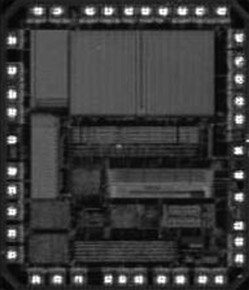
A smart tag is made of a flexible substrate, which serves as an antenna and a carrier for a flip chip (FC). In case of a contactless card, the flexible substrate with the FC is embedded in a card size piece of plastic. The two active ones of the FC’s three or four bumps are interconnected with the antenna. The antenna not only enables the communication with the chip; it also serves as power supply. Today, the most common FC/flex substrate interconnection technique is isotropic conductive adhesive (ICA). The antenna can be printed as a polymer thick film (PTF) onto polyester flex.
Since the placement accuracy requirement is relatively low, a high-volume/low-cost production can be realized with advanced flip chip shooters. A low-cost assembly is required as the target costs for disposable smart tags are in the range of a couple of cents.
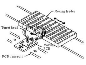
Traditional chip shooter
A chip shooter is determined by a horizontally rotating turret head, which simultaneously picks the components from amoving feeder bank and places them onto a moving PCB (figure 1). Thus, very high theoretical placement rates in the range of 40.000 cph are possible. For high-speed assembly of smart cards and RFIDs, traditional chip shooters cannot be used. These are the reasons why:
• No pick-up out of matrix trays (waffle packs) and from wafer
• The only feeding format is standard embossed tape (too costly)
• Placement accuracy is critical, typically clearly higher than 100µm at 4-Sigma(75 µm/3-Sigma)
• Integrated conductive adhesive application not possible
• Due to moving PCB no integration ofreel-to-reel transport
• Dynamically moved substrate can be critical for positional stability of flip chip
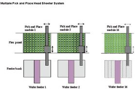
Within such shooter systems, 16 independent pick&place heads are typicallyarranged in a serial configuration (figure 2). Since 16 heads can work in parallel, very high placement rates in the range of 100,000 cph and more can be achieved. Most important for this throughput is a very high number of components on the panel. As this is definitely not the case in smart card/RFID panels, these types of shooters are excluded. Other knockout criteria would be such, as 16 wafer feeders are too costly, and placement accuracy of >100µm/3-Sigma is very critical.
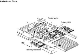
In the collect&place shooter system (figure 3) each of the two revolver heads are carried by a XY gantry. Thus the revolver heads, equipped with 6 or 12 nozzles, have random access to waffle packs (matrix trays), which also might be used for prototyping. Such systems are specified for 90µm/4-Sigma (corresponding to 67,5µm/3-Sigma) XY placement accuracy and a maximum of 20,000 cph. This placement rate applies for the standard SMD package spectrum plus outline centered smart card/RFID flip chips. As smart card/RFID assembly in most cases is a pure FC application, the collect&place shooter works as a flip chip shooter.
Flip chips can be collected from wafer feeders that are installed on stationary feeder banks (figure 9 and 10). Feeder-like adhesive dip modules can be installed as well on these feeder banks. A key advantage of this approach is the stationary PCB (substrate), which guarantees that already placed components are not shifted as a result of inertia. A stationary placement area is also mandatory for substrates in tape format (reel-to-reel). By the second half of 1999, high-performance flip chip shooters, equipped with two direct-chip-attach revolver heads, will appear on the market. Then, high-speed mounting of FCs based on bumps with a diameter of 110µm in a pitch range of 200µm will be possible.
For the majority of smart card/RFID applications, where the bump pitch is in the range of 0.8mm or even more, the placement accuracy of 67,5µm/3-Sigma of a collect&place shooter is sufficient. If the placement accuracy has to be higher, a high-performance shooter can be used.
Vision technique for component and board
A central aspect of modern SMD placement systems is the vision technique. Such a vision system generally consists of a PCB anda component visionsystem. Fiducial recognition with a down-looking PCB camera in smart card/RFID manufacturing is an important but not critical issue. The number of fiducials required depends strongly on the flex panel quality (non-linear distortions) and size. In the ideal case two fiducials are sufficient. If the non-linear distortions over a very large panel (450mm x 500mm) are too high, it might be necessary to divide the placement area into a number of sub-areas (for example 4). To each of these sub-areas, two individual fiducials will be allocated. Working with significantly more than two fiducials will certainly slow down the placement process tosome degree. The capturing of one fiducial takes approximately 0.5s. Common fiducial shapes in SMT (surface mount technology) are circle, diamond, cross, and square. In smart card/RFID panels, the antenna terminals (flip chip pads) can also be used.
To meet the demands in advanced SMT for strongly varying materials and surface properties with flip chips and other area array packages, extremely powerful component vision systems are required. Component vision system capabilities depend on both lighting (camera) technique and algorithms. Since FCs for smart card and RFID applications have relatively large bump pitches, the placement accuracy and thus the component vision requirements are much lower. Optical outline centering using front or backlighting should be sufficient. The slightly negative impact on placement quality, presented by wafer sawing tolerances (about 25µm), is acceptable.
If upcoming designs will include much finer bump pitches, a FC bump centering might be necessary. To eliminate flip chip sawing tolerances, bump centering is mandatory. Vision bump centering is only possible with a frontlight system. A maximum of recognition reliability can be achieved by means of a sophisticated, flexible lighting technique using various light sources. Each light source is determined by a specific emission angle. An adequate contrast between the relevant structures (bumps) and the interfered background environment can be attained. A high variance in lighting can be provided by using at least three different light sources. A maximum of flexibility exists when the intensity of each light source can be programmed in fine increments. A library contains the individual, ideal lighting for each package.
The quality of the flip chip image (figure 4), captured by a specific camera, is nearly perfect. The slightly visible routing structures can be easily suppressed by the bump find algorithms. For bump centering of the sometimes very challenging area array packages, algorithms suitable for standard SMDs can scarcely be applied. Therefore, time-consuming but very interference tolerant contour search methods are more advantageous.
Feeding the chips
Basically, for flip chips three feeding methods can be used. The embossed tape is principally ideal for SMT high-volume production but the die-sorting and tape material costs are not acceptable for theextremely cost-driven smart cardsand RFIDs. The 2 x 2-in matrix tray isvery common in the bare die area, and is ideal for low and medium volume and/or high component diversity. For high-volume/low cost needs it is not suitable. For smart cards and RFIDs it seems only acceptable for prototyping. Bare diefeeding directly from the wafer must definitely result in lower component purchasing prices due to the eliminated die-sorting job.
Wafer feeding is the clearly preferredfeeding method for smart card/RFID.There are three ways, called stationarysystems, feeder modules and flexible wafer handling. With stationary systems, integrated in the feeding area, the dies can be picked-up directly by a placement head. Time-consuming die pick-up will cause a significant throughput derating. The flip operation in case of bumped die makes the whole placement process slower and more complex. Under certain conditions, a stationary system integrated in the feeding area can be a good solution.
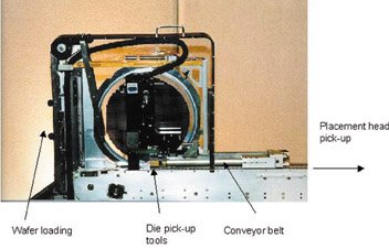
A wafer feeder module (figure 5) can be considered to be a complex SMD placement machine feeder for one type of die. The wafer is loaded manually from the front side. Loading and processing is carried out in a vertical orientation. The dies are ejected, picked up and placed onto a conveyor belt. Depending on the bare die technology, applied in the placement machine, the dies can be placed onto the conveyor either face up (for COB) or facedown (flip chip). The pick-up rate of the machine’s head can be much higher than the die delivery rate of the wafer feeder as emptying and refilling the conveyor can be done independently. For example, after having picked six bare dies, a revolver head moves away for collecting other components and finally placing the complete load on the board. In the meantime, the wafer feeder can refill the conveyor. To enable high-volume FC-based RFID manufacturing, two or more wafer feeders can be installed on the feeder banks of a flip-chip shooter.
A key feature of a flexible wafer handler is the capability to execute a wafer magazine. The dies from a wafer are placed onto atablet, which can be moved into the access area of the placement head. Depending on the bare die technology applied, the dies can be presented to the placement head either face up (COB) or face down (flip chip). The flexible wafer handlers are, with price and floorspace requirements, in the range of a die bonder or SMD placement machine. To allow for the highest pick-up rate, a dual gantry shooter for smart cards/RFIDs with two or even four wafer handlers will be required. Such requirements render this solution not suitable.
Conductive adhesive
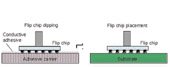
Isotropic conductive adhesive (ICA) application will gain tremendously in importance, as this seems to become the dominating interconnection technique for smart cards/RFIDs. The adhesive dipping process is considered to be a flexible, low-cost alternative to stencil printing. The adhesive carrier is typically a rotating drum on which a thin film of adhesive is applied (figure 6). The additional cycle time per FC in a flip chip application like RFID is about 0.2s. Conductive adhesive dipping in conjunction with collect&place revolver heads is cost-effective and fast.
Some investigations were performed at Fraunhofer IZM in Germany, where an advanced placement machine Siplace 80 F+ equipped with a dip module was used for the application of adhesive. The dispenser was an Asymtec Millennium FCOBO,the reflow/curing oven an Heraeus (epm/h+e) Inertflow:
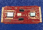
• The flex-based Espanex substrate was structured with Fraunhofer IZM test layout for the evaluation of FC processing using adhesive joining technology (figure 7)
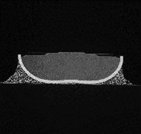
• The IZM test chip had peripheral bumps (pitch 200µm/300µm) of electroless-Ni with a height of 45µm as an underbump metalization and a goldflash, yielding bumps with a height sufficient for adheSsive joining.
• Conductive adhesive was Polysolder LT (Alphametals), which is a silver-filled epoxy formulated to replicate the junction stability and bonding characteristics of solder for SMT applications on non-noble metal finishes. It is capable of curing in standard profiles or at temperatures as low as 130°C.
To improve the process, the dipping module was used to apply conductive adhesive by dipping the flip chips into a thin layer of adhesive before placing the dies on flexible substrate. The thickness of the adhesive layer was optimized by a visual control of the transferred adhesive before placement. Different speeds of the placement machine were used to evaluate its influence on placement accuracy and interconnection quality. Shape of the bumps, quality and repeatability of the placement was investigated by additional cross sections of ICs after curing. As the gap height with the joined flip chips is rather low compared to soldered ones, the use of specific unfilled underfiller is necessary. But here, only the dipping process was investigated, not the underfill.
The optimum thickness of the adhesive film was determined to be 25µm for Ni-bumps with a height of 45µm. Figure 8 shows a thin layer of adhesive between flip chip bump and substrate, and gives an impression of the well-shaped adhesivereservoirs around the bumps, which is a prerequisite for high reliability. An influence of the placement speed on quality of the assembly was not detected, due to the intelligent Z-axis control, which slowsdown speed to minimum immediatelyprior to pick-up, dip and placement position. The placement speed was always set to maximum, yielding high quality interconnections as depicted below. The investigations revealed a stable process.
Shooter machine configurations
With two shooter configurations we are handling large flex panels of dimensions up to 450mm x 500mm with a carrier. Before placement, a support/fixing device is brought in contact with the flex panel underside. The device can, for planarization reasons, apply vacuum to defined areas on the panel. Another typical requirement is the flip chip presentation from a wafer.
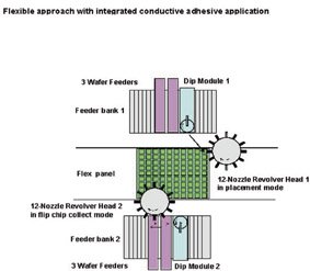
Figure 9 shows a flexible approach, which does not require an adhesive printing machine. The process sequence is as follows: A revolver head collects 12 flip chips from two wafer feeders, than moves over to the dip module and carries out a sequential adhesive dipping with all flip chips. Each bump structure is dipped into the film of conductive adhesive at different positions on the drum (flux spender). During the sequential dipping the drum (disk) stands still. After this, the head advances to the flex panel for placing the chips. At thesame time, at least one rotation of the drum is done to planarize the adhesive film. Having finished, the head moves back to the feeders for picking the next chips. These steps will be completed alternatingly with both heads. The practical throughput of the configuration will be in the range of 6,500 units/h (including secondary times and adhesive application).
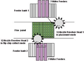
When we look for an approach for highest throughput having lower flexibility and needing higher equipment invest, wecome to a solution similar to figure 10. Here the adhesive application is realized with a screen printer or a pin transfer machine that is located in front of the shooter. The practical throughput of the configuration will be in the range of 11,000 units/h. In case of smaller antenna circuits the number of placements per panel will increase and as a result of this the throughput will also increase significantly. To achieve the maximum throughput, the flip chip shooter will require six wafer feeders in total.
Fax +49 89-7222-34001
Zusammenfassung
Wenn sich die Prognosen bewahrheiten sollten, gibt es sowohl für Smart-Cards als auch Smart-Labels auf HF-Basis demnächst einen riesigen Bedarf. An der Flip-Chip-Technik wird hier wohl kein Weg vorbei gehen, selbst wenn das einzelne Teil nur wenige Cents kosten darf. Der Fertigungsprozeß steht somit unter hohem Kostendruck und muß daher absolut effizient erfolgen.
Résumé
Si les prévisions s’avèrent exactes, les Smart-Cards et les Smart-Labels sur base HF feront bient’t l’objetd’une demande énorme. La technique Flip-Chip sera probablement incontournable, même si chaque composant ne doit coûter que quelques cents. Le processus de fabrication est donc soumis à une forte pression des coûts et doit être d’une efficacité totale.
Sommario
Se le prognosi dovessero avverarsi, sia per le Smart-Cards che per le Smart-Labels basate sull’alta frequenza, prossimamente subentrerà un notevole fabbisogno. Pertanto non si potrà fare a meno della tecnica Flip-Chip, anche se il singolo componente deve costare soltanto pochi centesimi. Per questo motivo il processo di produzione si trova sotto elevate pressioni di costi e deve pertanto avvenire in modo assolutamente efficiente.
EPP 235
Unsere Webinar-Empfehlung
Die Nutzung der 3D-Mess- und Prozessdaten bringt die Produktionssteuerung auf die nächste Stufe. Echte 3D-Messung ermöglicht KI-basierte Prozessmodellierung zur Vorhersage von Parameteränderungen und -defekten oder zur Ursachenanalyse bis hin zu einzelnen Werkzeugen und Best…
Teilen:


