Lead is an essential part of alloys used for soldering. The EU directive that would have initially forced us to eliminate leaded solder alloys has now been postponed until 2008. This final part of our series is concerned with context and consequences that arrive from all relevant steps in the entire process chain with their interactive be-havior.
Rolf Ludwig Diehm, Seho; Werner Kruppa, Multicore; Armin Rahn, rahn-tec
The user scenario:size is determining
The discussion and most of the research about lead-free has been carried on so far by representatives of relatively big businesses and big organizations. However, in reality we again face that well-known proportion of 80/20 that we are prone to regularly encounter. 20% of large companies produce approximately 80% of all electronics, whereas 80% of little companies sign responsible for the remaining 20%. And who is to say which products are more important? The lead-free legislation will, however, bite everyone with equal vehemence. The problems that these two groups will have to face are of an entirely different nature. Whereas the ‚little ones‘ have to wrestle with their limited capacity in resources, the ‚big ones‘ have programs to certify solders, fluxes and individual processes. Nevertheless, it is doubtful that by 2008 they will have sealed all the details.
The information that we presently have available is based on very limited research. Production tests like the one carried out at Nokia (in cooperation with Multicore) relate only to a very narrow number of instruments. Such experiments make a definite basic statement, however, opening the way to more questions than they actually solve. Tests such as the ones performed at the Technical University of Munich (Dr. Wege), are equally useful. But, because of their ‚laboratory nature‘, it is extremely difficult to translate them into a mass-production environment. There are already some manufacturing lines based on lead-free technology. Basically, it is possible to switch to lead-free – at least in some well-defined cases. If, however, then the entire electronics industry must change over.
The imponderable part that we refer to relates less to the individual materials such as solder, flux, components and PCB. Where we identify a lack of knowledge is in the area of interactive behavior of all these players in the process. Each such factor carries more than a dozen parameters, and potentially, they all may interact or even react with each other. As may be seen from statistical investigations: Such situations become quickly unmanageable. Or they develop into such cost avalanches that most of the potential influences are neglected and thus not investigated. The long-term risk is evident.
The result of soldering should be a reliable electrical connection within the limitations of the process. Up to a certain level of confidence, this may even be tested. Nevertheless, in order to make inference, the precise parameterization has to be laid down. Otherwise, it would be impossible to deduce the cause of an early failure. Today, with lead-bearing solders, we are only at the very beginning of understanding these correlations.
To develop such a lead-free program sounds very ambitious. At least it looks as if we were ready to map out such research. But on closer examination, we are not yet prepared. The legislators have not yet defined all the terms of their efforts, and, therefore, many of the basic facts of ‚what we have to do‘ are so far not clear (seepart 1). Neither has there been any decision about the alternative solders (part 2). Furthermore, the definition of the process has hitherto not been forthcoming: times, temperatures, surface finish, permissible residues, soldering methods, etc. There is a lot of work ahead before we can actually concern the research labs with reliability issues and test procedures.
The process:three prime methods
For lead-free procedures, there are mainly three methods of interest: wave (flow), reflow and selective soldering. These three technologies are distinctly different and pose very diverse problems. Hence, they should be discussed separately. We may also point out that in reflow, the type of energy transfer again subdivides this process.
There are a number of common elements among the soldering methods, and we place those at the beginning. Paramount among those is all the topics that concern themselves with the PCB and the components. This leads into discussions about subject matter that has not even been solved by everyone for traditional soldering methods. When carrying out unofficial surveys, we find regularly that such aspects as cleanliness of PCBs or their solderability are not even specified in purchasing contracts. Questions relating to solder mask material and their application or curing are not discussed either, despite of the fact that they are critically involved in the creation of solder balling.
Questions that relate to PCBs are relatively easy to manage, partly because these usually relatively small PCB shops are quite responsive to customer requests. On the other hand, component manufacturers are generally very large corporations not exhibiting great flexibility. In addition to these, we have some misgivings about norms: They do exist but often are not tight enough to make life easy for users.
It may be opportune to make some cautious assumptions with regard to new solders. We may be relatively safe in assuming that:
• The melting point of any new solder will be higher than that of Sn63Pb37
• The lead-free solders will have a higher tin content, and will be lighter because of it
• The present fluxes will have to be adjusted to some extent
The PCBs:very critical items
The following aspects of the PCB may give cause for reflection: substrate material, surface finish and the solder mask. When contemplating the substrate material we are in a relatively favorable situation. Even now, we have a large selection of different standard substrates at our disposal. Alternatives seem to be available when we need them. As we are not yet sure at which temperatures our process will actually perform well, it looks a little premature to make a decision. When compared to FR4 (Tg of 125 to 145°C), we find that most alternatives are more thermally stable, but also more expensive. Some of the materials have produced difficulties during manufacturing. Micro cracking between reinforcing fibers and resin system are just one example. Other materials have raised issues such as health concerns for those working with them. The price of most is higher than that of FR4, and the ‚cheaper‘ ones seem to demand a premium of about 10%. If the user insists on even more stringent demands, he will have to face even higher cost. Demands for better dimensional stability and dielectric performance, tighter tolerances, lower contamination values, etc. could likely be carried over from FR4 and may even be improved in many cases.
When discussing the surface finishes of PCBs, our selection appears to be much narrower. There are a couple of aspects that need thought. As the pitch is getting smaller, we will have to request planar surfaces for printing and mounting. Especially in Europe the traditional hot air leveling (HAL or HASL) is prevalent. This solder dipping and hot-air-treatment process is, however, a very stressful experience for a substrate, and neither do they produce a planar surface. If lead-free HAL coatings are demanded, we may wave good-bye to FR4 as it is already challenged thermally and with regard to its stability. Even now we blame a lot of delamination of multilayers on the HAL process. It would be high time to carry out thorough tests on whether lead-free coatings using the HAL process are possible, and whether similar results with regard to storage and solderability may be achieved as in the case of Sn63Pb37. These questions may entail a specific choice of flux, and here the problem of residues raises its head immediately.
With this surface finish, we have at least the feeling that if HAL is possible with lead-free solders, then the further soldering process would not run into difficulties. With the increased tin content of solders,it may be possible that the tin-rich intermetalic (e.g. when storing for extended periods of time) may be counter-in-dicative. More tin usually means faster growth of the intermetalics, as more material is available for reac-tion.
Among the other surface finishes, those known collectively as organic pacification (OSP – organic solderability protection) have attracted a lot of attention lately. Planarity, environmentally friendly process, solder quality and low cost give these finishes a special attractiveness. They are however sensitive to elevated temperatures. As soon as the temperature climbs to 110 or even 120°C, they start to disassociate. We are still waiting for proof that these surfaces meet the requirements of individual process as to the necessary thermal demands of the soldering method, and that they are compatible with the alternative solders (special fluxes?). The fact that in the case of OSPs and 63/37 solder where nitrogen makes the process robust, must be verified for all those different lead-free solders once more.
Ni/Au may profit from higher temperatures during the process. Solderability problems that were encountered in the past often could be solved by jacking up the temperatures ‚a little‘. How alternative solder reacts to the ominous P in the Ni must, however, be explored anew.
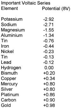
Whiskers are caused by minute electrical potential differences between the metals that are helped by small amounts of ionic contaminants and humidity. For tin-lead solders this behavior is reasonably well understood. In the case of lead-free, we will have to account for other oxides and salts (reactions of flux constituents with the metal oxides). A good part of these oxides and metal salts are water-soluble (those of silver) and thus particularly liable to help in the creation of whiskers. The use of other metals adds another element in this chain of events. Tin and lead are only separated by a potential difference of 0.01V, for tin-copper this difference increases to 0.47V, and for tin-silver even to 0.93V.
We anticipate that in quite a few cases only ensuring better cleanliness of the assembly after soldering will check the predicament. Considering the possible problems stemming from hot air leveling (perhaps increased residual contamination on the PCB as delivered) and a different chemistry in fluxes, the task of cleaning may loom at the end of the switch to lead-free solders.
Quality has two aspects that are generally mixed together thoroughly in order to befuddle the unwary user: reliability and defect rate. In the case of SnPb-solders, we just finished major research projects that verified that visual appearance (i.e. the traditional ‚defect‘) does not correlate with the reliability of the joint. Looking at the joint will not provide any clue to its ‚inner life‘. Is this true for lead-free joints as well? Can we just carry over the new-found definition of defects? According to IPC standards, we do not have to fill through-holes any more. The notorious 360° fillet is no longer required either. Not even all the bare metal has to be covered any more. Can we trust those recommendations in the case of no-lead technology? At least zinc-free base metal would be rather problematic. And we should not forget that due to higher temperatures we might have to work with different flux chemistry.
With regard to the reliability of lead-eutectic joints we now can fall back on a voluminous database. This real-life data forms the starting point for all those programs that simulate joint failures. In comparison, experience with no-lead alloys is quite limited so far. As we have learned that reliability data derived from experimental setups do not entirely correspond to field failure data, we will have to do a lot of work here. Data from bending and thermal cycling tests as well as those obtained from vibration experiments will have to be matched to actual failure reports. This will take some time, as we will have to produce first, deliver and wait before we can even think of establishing a pool of field failure data. Considering the multitude of test procedures and applications, many may look with sad eyes at the laboratories that just recently have been eliminated to cut overhead.
X-ray may be the only viable method (and ultrasound?) that permits us to look into a joint without destroying it. It is well known that the absorption capability of lead is a great simplifier of these methods. Such inspection methods are strongly recommended for components such as BGAs, SLICs and FCs. However, we still have a hard time interpreting those images that we get for lead-bearing joints. Information of how to fine-adjust the X-ray equipment, and how to interpret the images for lead-free alloys has to be forthcoming soon or we are in trouble here, too. Even if ‚defects‘ are observed, how do we judge their importance for the reliability of the joint? Who knows whether shadows that only indicated harmless phase changes within the joint for SnPb-solders are not fatal defects for Pb-free alloys?
Wave soldering:a valuable pot
It is well known that bismuth expands during cooling. It is thus difficult to remove bismuth solder from a casting form. Such limitations are encountered and make it hard to manufacture bar solder of such alloys. During wave soldering, we may encounter this property as well. The solder module cannot be shut down any more without running into the hazard of bursting the solder pot. Bismuth solder has to be kept liquid at all times. Shutting down the unit during the night or Christmas or during weekends is out of the question. This by itself adds considerable cost for additional power requirements when operating with bismuth solders. Furthermore, precautions against power failures are needed, too. When the power cable is severed in the neighborhood, one has to be ready to immediately drain the pot. Otherwise, cracking of its walls may be hard to avoid. It is not only the damage to the pot that one wants to avoid, but also the possible loss of solder and the ensuing mess should solder run out of such a crack.
Extensive studies have just been concluded that investigated the optimization of pad-designs. Naturally, the basis for such investigations was the traditional SnPb solder. It is pertinent to ask the question of whether these valuable results – and thus the layout recommendations – can be adopted directly or indirectly for lead-free solders? Especially when wave soldering, one could easily imagine that the weight difference between these two classes of solders may change the optimum pad design with regard to defect levels as well as perhaps even its reliability. The flow characteristic will be different. As we also have to crank up the temperature, we reduce the viscosity of our molten solder even further. The optimal pad design may be based on a different geometrical pattern.
When discussing solders, it has become customary to undervalue certain situations. One prefers to discuss the additional cost for solder on the basis of use-per-assembly. Even if we go to extremes and assume that the price of solder would double – which it definitely should not – the additional cost per assembly would be rather small. If, however, we take into account the cost of filling the solder pot, the situation and the angle of view changes suddenly. Whereas larger corporations will look at it as a necessary investment cost, smaller companies may face a serious condition. Whether the solder in the pot costs 4000 or DM 8000, this may produce more than just an amused scratching of the head.
Despite some publications to the contrary, we expect that solders with a high tin content will produce more dross than those with a lower percentage. Oxidation is thus another problem. As known from the respective literature, nitrogen is usually seen as the necessary ’savior‘. An atmosphere low in oxygen improves wetting and largely prevents the creation of dross. Expensive solder will create expensive dross. The cost for N2 is put into relation with the cost of dross. If a nitrogen installation already exists, the additional cost does not occur. But many systems still operate without nitrogen, and the cost for gas, installation, tank and any rental cost will enter into the calculation. The small user will find this a considerable burden. In total, the process will become more expensive: Because either the dross will become more costly, or because the necessary use of nitrogen will increase the cost picture – indications are that the nitrogen option will be cheaper and thus preferable.
Tin is an aggressive medium. Therefore, it has a tendency to form bimetallic compounds with a great number of other metals. The higher the tin content and the higher the temperature, the more this property will manifest itself. In hi-temp soldering applications we have regularly observed that pumps and other movable parts are preferentially attacked. Movement, mixing and a certain friction act together and further leaching of metal parts. Even stainless steel [V4A – 316] may last only few months before it practically’disappears‘. In some cases, even titanium failed in the long run. Most coatings that were tried offered only limited protection and wore off quickly. If we have to fall back onto specialty steels, the cost for solder pots, pumps and related hardware would skyrocket. It is not rare that such solder units cost as much as an entire soldering system. Part of the cost would be the exotic metal, however, and part of it would be due to the difficulty of cutting, machining and welding. Such steels can only be welded by specialists. Expensive cutting steels are often ruined after only 1000mm of milling.
At this point, such examples are extreme. However, before we do not know precisely which solders and which fluxes and at what temperature all this is going to happen, such potential equipment aspects should not be discarded altogether. Little research has been done on such wearing of movable parts in a solder pot. We have little information on how they could affect the process. Occasionally, one encounters observations about wave crest stability in such companies that pursue a ‚zero-defect‘ strategy. As they try to control all parameters, they may come to realize that pumping changes with time. Whether such fluctuations in wave crest behavior or flow height is due to dross accumulation, a change in the tolerance of the pump would have to be checked in each individual case.
Immediately after the introductions of low solid fluxes and the use of nitrogen in Germany, two large investigations were carried out regarding the occurrence of solder balling. Both came to the conclusion that the main factor was the solder mask. How they explained these findings differed considerably from one such study to the other. These analyses limited themselves to traditional lead-containing solders. Which role lead plays in this equation was not made clear. It is only expected that someone wants to ask the question whether there are significant differences in the behavior of lead-bearing and lead-free solders as to reactions with solder masking material and the formation of solder balls. It would be welcome news if the pendulum would swing once into the otherdirection, and that the new solders would be less likely to cause solder balling.At this point, however, we are not yet in the position to make such a rash state-ment, as nobody seems to have checkedit. As there are other reasons for solder balling on an assembly, these fields will have to be looked at, too. How about solder splatter from the soldering unit? Inaddition, one would have to investigate the mobility of such solder balls. Is therea change compared to adhesion (tin content), or are they displaced more easily (difference in weight and density)?
Our knowledge about contaminations in SnPb solders and their effects is very limited. Comparing different sources with regard to allowable levels of contamination has shown that they are either copied from each other (with minor modifications to make it less apparent), or that there are very few fundamental researched articles [cf. the work by Dr. Thwaites, TRI]. In the case of lead-free solders, the results of a literature review was even much more meager. Little is known about contamination with lead, but otherwise one comes up practically empty. This is not surprising as investigations into these boundary conditions of the new alloys are particularly involved and difficult. If we cannot agree on the melting point of such alloys, how could we be more precise with regard to minute shifts in composition or small amounts of foreign material? Our knowledge about the behavior of SnPb solders is based on long years of production experience and such numbers are not yet available for Pb-free alloys.
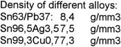
At this point, we may also address the question of ‚runaway tin‘. When using 63/37 solders we regularly observe that the proportion of tin in the alloy starts to decline – mostly due to the generation of dross. These solders are very robust against minor deviations. Whether we work with 60/40 solder or 63/37 is hardly noticeable. It is also quite easy to calculate how much pure tin has to be added in order to bring back the original composition. Whether this shift in tin content is faster in Sn96,5Ag3,5 or Sn99,3Cu0,7 and whether it would be more critical, is still unknown. Looking at the phase diagram, one would think that, for example, a change in the melting point would occur more quickly than for SnPb. The liqui-dus lines are steeper than for tin-lead solders.
Reflow soldering:many windows
Pastes are a rather complex concoction where many parts play an important role. On the one hand, we have the constituents of the paste, and on the other the many’windows‘ during their use. The former determine the pastes‘ properties, the latter the result during production. Matching them well is the key when trying to optimize a SMT line.
If we can trust the statements of relevant specialists, the manufacture of consistent charges of solder paste is not without its intricacies. In many cases, it may depend on the fact that the one who mixes it does not really control all quality aspects of the ingredients: The monitoring from birth to death is lacking. Most paste manufacturers have delegated the production of solder powder to specialists. Thus, they have no real influence on form, size, distribution or even the oxide content.
Powder is one of the items that determine the printing properties of the paste. The other ones are the carrying and the thixotropic agents. On the other hand wetting is established by activators. The type of lubricant defines form stability and slumping during heat-up. It also signs responsible for the susceptibility with regard to humidity as well as the sensitivity to increases in temperature during processing. Whether flux manufacturers will have to change some of these chemicals to meet demands for no-Pb solders or not will soon become known.
Because of the higher process temperatures, we expect that some of the Pb-free solders may demand a change in the acid systems of our fluxes. So far, the carbonic acids have served very well. However, they are not necessarily the most thermally stable chemicals. The amount of oxides that can be tolerated in a powder (it will increase as the tin content of the powder will be substantially higher) depends on the type of acid and its total percentage in the paste. This will be decisive, as it will establish which surfaces we will be able to solder and how much aging of them we might be able to tolerate.
The users have a slightly different perspective. They are concerned about the quality of delivered pastes, their storage capability and conditions. During processing they look at slump, process windows and the behavior during printing. Furthermore, they want to know what reflow profiles would be suitable. As all the chemicals in a paste are stored together with the metal, chemical reactions are at least potentially possible. The higher the activity of the ingredients such as acids, metals, oxygen, etc., the higher the probability that the paste’s properties will change between the dates of manufacture and of use. If this period is extended and the temperature high, the more likely reactions will occur. A high tin content and more aggressive acid may contribute to a decline in storage time.
If the resin system is changed, this may have direct implications for the printing properties. The printing process is presently seen as a general bottleneck during production. Hence, we observe the effort to develop speed printing pastes and systems. It is obvious that the paste manufacturer is called upon to ensure that a new formulation conserve this valuable aspect. Whether we can keep the metal content at 90% or above will be seen.
The problem of solder balling during reflow has a different causality than when flow soldering. One possible trigger is the softening of the paste during heating or even a capillary drift during melting. Whether the advances that we have seen in this regard for our traditional solders can be replicated for lead-free ones, is still uncertain.
Depending on the gT of the assembly, the thermal profile used during reflow either exhibited a plateau or not. Many of those pastes used today are suitable for either one – although most would prefer a direct heating without an extended dwell period before the peak. If higher reflow temperatures are now needed, the problem of the gT will be intensified. The time above liquidus and increasingly the time above the Tg will have to be examined more closely. The new demands made on the pastes and on the equipment become rather clear.
For example, convection reflow machines have proven to be particularly prone to failure of moving parts. Should motors and bearings find themselves in the hottest part (above – heat rises), they need active cooling or their reliability is endangered. Experience has taught us that preventive maintenance is often required. If we have to increase the internal temperature, the problem will escalate. Even today, such blowers perform already at their thermal limit.
For some pastes, the soiling of the inner chambers of the equipment is hard to control, even with advanced flux trap designs. These problems are particularly urgent in mass-production environments when three shifts hardly leave time for service. With new pastes, this maintenance problem may be intensified. Add to this the potential increase in aggressiveness of the activators, and we have the added demand for acid resistant inner coatings of the process chambers.
Selective soldering,repair and design
For selective soldering, in the case of dip or drag methods, one of the critical parameters is the distance between the assembly and the solder. Increased soldering temperatures may contribute to the warping of the laminate (pre-heat). Supporting the assembly during soldering (dip), and improved design of the gripper system will certainly counteract such potential problems. However, there is a need for more practical experience in mass-soldering applications.
For repair, replacement solders will also affect the scene. Compatibility of solders will be essential. Mixing of solders cannot be recommended. A well-known phenomenon is the lifting of pads due to too much pressure of the tip on the pad, or too high a solder tip temperature. The higher melting point of Pb-free solders will require higher tip temperatures. We will have to be more careful about temperature settings as we have to make sure that the adhesion of the Cu cladding is not endangered.
Contamination of the assembly due to repair has always been an apprehension. We may have to rethink our approach. Activators that are more aggressive will be the cause. Wiping with the alcohol cloth is surely not enough if high demands are put on cleanliness. Moreover, we have to hope that our choice of lead-free solder is available as wire. Because of a lack of malleability, solder wire is not available for some of the potential no-lead alloys. Should the flux core become unavailable, we would have to make do with other methods of flux application during repair. This may slow us down, but it won’t shut us out.
In the design area, the no-lead discussion has brought other topics to the fore. Alternative joining methods will certainly widen their respective niches. Conductive epoxies are a prime candidate. Press-fit, a technology that has suffered a certain lapse of popularity, may be looked at somewhat more favorably again. Particularly interesting would be all those processes that can do without flux. Two plasma processes have reached the market already. A third method is actively developed in the US. Rockwell is working on a chemical reducing procedure that would be substantially different from fluxing. Activated water vapor is discussed in Germany. A French invention is of special interest as it is based on dynamic activated gas reduction principles.
All of the methods refer to flow soldering only. Here, major breakthroughs seem to be more evasive due to a key difference of the fundamental situation. Some beginnings in this direction can be noticed even for this major growth area. However, more work is required if we are to be convinced of their effectiveness.
Concluding remarks
Perhaps we should make some final statements about all those metals that are to replace the dangerous lead. Investigation of the environmental acceptability of such solders (SnAgCu, SnAg, SnCu and SnSb) discovered that (water) leaching of such metals could be very high (for Sb 10.000 time above the value set by the EPA for drinking water). The authors arrive at the conclusion that‚ if solders which contain silver or antimony are not properly discarded, should they meet groundwater, they would make this water unusable according to EPA standard. What is true for solder is certainly true for dross. The authors think that lead-free solders are no cure-all if we look for a solution to the potentially toxic effects of SnPb solders.
The feeling which seems to be spreading that only lead is problematic and all the replacement metals are safe, is wrong. It is true that the US Agency for Toxic Substances and Disease Registry has placed lead with 1522.67 points right after arsenic in position 2 of their list of the 1997 CERCLA Priority List of Hazardous Substances (containing 275 items). But: Nickel with 1004.94 is number 49, zinc with 802.36 points occupies position 65, bismuth-214 with 802.36 occupies position 131 (just after plutonium in position 126), copper with 797.77 makes it into 136, silver with 611.15 takes 196, and antimony with 572.91 points occupies position 241. In other words: We find all the ‚other‘ metals on this list too. Further information and an explanation on how this list and its point system was arrived at may be obtained from: ATSDR Information Center, Division of Toxicology, Mail Stop E-29, 1600 Clifton Rd, NE, Atlanta, GA 30333
EPP 151
A three-part series
In the first part (EPP Europe issue #4/2000), we discussed the environmental and legal situations for the switch to lead-free manufacturing. The piece II (EPP Europe issue #7/8-2000) has dealt with consequences that arrive from metallurgical considerations. For example, which alternatives do we have? In this final part, we have brought all relevant process considerations into context.
Literature
R. Rasp: PCBs – an Outlook; Presentation: Technical Program. Nepcon West ’99, Anaheim, California, 1999
M. Racic & S. Goodell: No-Lead and Horizontal Hot Air Leveling. Proceedings of the Technical Program, Nepcon West ’95, Anaheim, California, 1995
L. Hymes: Recent Concepts and Solutions in Soldering Technology. Proceedings of the Technical Program, Technical Session 32, Nepcon West ’97, Anaheim, California, 1997
German Joint Project: Reliability of Solder Joints SMD-PCB in the Range of Inspection Criteria Limits. VDI/VDE-IT
H. Schmidt: Seho Technology Day 1999
A. Rahn, R. Diehm, E. Beske: Bleifreie Lote; Productronic 2, 1995
E.B. Smith III & L.K. Swanger: Are Lead-free Solders Really Environment Friendly? SMT; March 1999
Zusammenfassung
Die Diskussion um die EU-Gesetzgebung zur Verbannung von Blei aus Elektronikprodukten schlägt hohe Wellen. Wobei derzeit immer noch Lücken bestehen, beispielsweise wie ist „bleifrei“ definiert bei mobilen Geräten mit Bleiakku zur Spannungsversorgung bzw. bei Fahrzeugen mit voluminösen Batterien ? Dabei wird die Zeit allmählich knapp, insbesondere für Großunternehmen, in denen die Umstellungsprozedur lange Wege zurücklegen muß. Nachdem vom globalen Blei-Jahresverbrauch lediglich 0,5 % auf die Elektronik entfallen, stellt sich natürlich die Frage, was passiert eigentlich mit den restlichen 99,5 % ? Ironisch formuliert: Wirken sich diese nicht auch toxisch aus?
Résumé
La discussion autour de la législation européenne visant à bannir le plomb des produits électroniques fait des vagues. Des lacunes continuent de persister par exemple sur la façon de définir l’absence de plomb dans le cas des appareils mobiles alimentés par des accumulateurs au plomb ou des véhicules équipés de grosses batteries au plomb. Or le temps presse, notamment pour les grandes entreprises dans lesquelles le pro-cessus de conversion est complexe. Dans la mesureoù 0,5 % seulement de la consommation totale de plomb est imputable à l’électronique, on est bien sûren droit de se demander ce qu’il en est des 99,5 % restants? Ou plus ironiquement, ne sont-ils pas toxiques, eux?
Sommario
La discussione riguardo alla legislazione europea per l’eliminazione del piombo dai prodotti elettronici fa molto parlare. Infatti vi sono ancora molti concetti poco chiari come per esempio la definizione di „senza piombo“ nel caso di apparecchi mobili con accumulatori di piombo per l’alimentazione di tensione oppure in caso di veicoli con grandi batterie al piombo. I tempi diventano sempre più stretti soprattutto per le grandi aziende in cui il processo di trasformazione richiede molto tempo. Se si tiene conto che il consumo annuale mondiale di piombo ricade solo per lo 0,5 % sui compo-nenti elettronici, ci si chiede naturalmente cosa succeda con il rimanente 99,5 %. Per formularlo in maniera ironica: non è nocivo anche il resto?
Unsere Webinar-Empfehlung
.png)
Auch dieses Jahr präsentiert Koh Young wieder aktuelle Trends und „State of the Art“ Technologie aus der optischen Inspektion und 3D-Messung auf der Productronica in München. Aber wir alle kennen das Problem voller Terminkalender, Reisebeschränkungen oder fehlender Zeit, um in…
Teilen:


