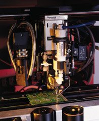


Although wire bonding dominates the IC packaging market in volume, most of the industry „buzz“ has focused around advanced techniques, such as chip scale packages (CSP) and flip chip (FC). They represent only a small portion of the overall volume, but analysts are predicting rapid growth because they represent the most viable path for achieving high-density requirements. We will take a closer look at the underfill dispensing which has helped to make the technologies production-ready.
Steven J. Adamson, SemiconductorPackaging & Assembly Product Manager, Asymtek, Carlsbad, CA
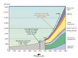
Electronic Trend Publications have, for example, predicted that CSP usage will grow from its 1997 level of 158m units to just over 1bn in 1999, reaching approximately 3.9b in 2002, representing a 90% annual growth rate. Similarily, Prismark Partners has estimated that the number of FC units increased by 40% during 1998, to a total of 899m. While the combination of CSP and FC volumes still comprises only about 2 to 3% of more than 60bn ICs produced annually, it is clear that these technologies will pull significant market share from traditional wire-bond methods.
However, even these growth forecasts for FC and CSP represent something of a scaling back from the extremely bullish predictions of just a few years ago. As with many new technologies, where the initial optimism out-strips the practical implementation considerations, both FC and CSP have had to undergo a significant maturation process to become ready for production. The need to invest in equipment and methodologies has also tended to make IC manufacturers opt for squeezing the maximum results out of their existing wire-bond techniques before changing over to other technologies.
In addition, the introduction of flip-chip on board (FCOB) appears to have been deferred somewhat because a number of manufacturers have focused instead on CSP implementations as a potentially easier transition and then have reconsidered as they encountered unanticipated production and design challenges.
The tradeoffsbetween CSP and FC
Many manufacturers initially saw CSP as something of a softer entry than jumping directly into flip chip, because it appeared that much of their existing surface-mount equipment could be transitioned to CSP. Because the task of putting a CSP onto a FR-4 assembly was essentially the same as any other SMD, CSP represented a very attractive interim step that did little to disrupt the efficiency of mature SMT production lines. Also, since the definition of CSP calls for about 20% more the size as the die itself, it appeared to come close to providing the densities achievable with flip chip, while allowing for more latitude in the board level processes being used.
From a cost and difficulty standpoint, controlling the quality of a relatively small CSP interposer substrate was considered to be significantly less daunting than the challenge of trying to control the substrate characteristics and precision microvias for placing a flip chip directly on the PCB assembly itself. According to the National Electronics Manufacturing Initiative (NEMI), organic PCBs account now for more than 90% of interconnecting structures, with FR-4 representing 85% of the resin system used to produce copper clad laminate. Current organic PCB technology has already climbed the volume curve and descended the cost curve to the point where it has become viewed as a bedrock technique that should be leveraged rather than displaced or disrupted.
In addition, when it comes to layout of interconnects, CSP allows for significantly larger circuit trace and spacing dimensions than FCOB, thereby making it more compatible with PCB trace size in the 100µm range. On the other hand, cost of the substrate could be significantly driven upward by the laser-drilled microvia tech-nology, and 50 to 75µm trace dimens-ions that are typically required for FCOB applications.
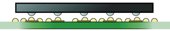
There was also widespread belief that the more controlled substrate conditions and larger solder ball dimensions in CSP would provide the required mechanical stability and thereby avoid the need for using underfill processes. Because CSP solder ball heights run in the range of 12 versus 3mil for flip chip, early CSP designers knew that the solder ball structure itself could handle the mechanical strains associated with thermal expansion of the substrate and die. However, it has been shown that CSP reliability due to mechanical shock needs to be significantly enhanced through the use of underfill. Therefore, effective underfill dispensing plays a key role in both CSP and FC applications, but for different failure mechanisms.
Densities are drivingtoward flip chip use
Over the past few years of real-world experience, manufacturers have painfully discovered that CSP is not just a „drop in“ on their existing SMT lines, but also requires the learning curve, process adaptation and equipment investments associated with any major technique. At the same, the relentless push toward greater densities has also driven many of these manufacturers to take a closer look at applying what they’ve learned and making the jump to flip chip.
For most consumer electronics, ever-increasing densities have been accepted as form factors become smaller and functionality rises for cellular phones, pagers, digital cameras, handheld computers and other high-volume items. In many cases, CSP designs are becoming so tight that the dies are almost touching each other with virtually no spare real estate left on the board. As a result of this continued march to higher densities, the general feeling in the industry is now shifting to view CSP as just a step on the way to flip-chip technology, with a useful life of only 5 to 7 years.
Dispensing optimizationfor CSP and flip chip
Even though in the longer term, CSP may be viewed as a transition technology, it is important to harvest everything from the process that has been learned to date to effectively apply the best techniques to meet the ongoing challenges of process control and optimization. For example, accurate dispensing of encapsulant underfill has become a key component in the reliable manufacture of both CSP and flip-chip devices. System suppliers and fluid formulators have worked closely with FC andCSP manufacturers to improve processes, such that dispensing capabilities have already progressed to a third generation of refinement.
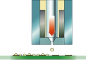
For example, flip chip in package (FCIP) designs such as ball grid arrays have already driven dispensing techniques to a high level of sophistication and process control to achieve consistent underfill beneath the die, while avoiding voids or overflow of material. In flip-chip underfill applications, precision control becomes a concern because the dispensing needle has to move close to the chip throughout the process. The needle must be positioned far enough from the chip to avoid backside contamination but close enough to promote capillary flow of the fluid under the chip. In addition, the dispensing pattern must be carefully designed to optimize flow-out under the chip while maximizing throughput. Although throughput considerations often require dispensing on multiple sides of the chip in a single pass, extreme care must be taken to manage the flow-out directions of multiple wave fronts that are created under the chip. The angle of intersection between multiple wave fronts can be a major factor in the creation of voids. By controlling the dispensing pattern so that the wave fronts merge at an oblique angle of greater than 90°, the likelihood of voids can be significantly diminished. However, if opposing wave fronts meet at an acute angle of less than 90°, the risk of creating voids is greatly increased.
In the early use of CSP technology, almost no one felt that underfill encapsulation would become a significant requirement. However, empirical experience and increasing densities have led most CSP manufacturers to incorporate underfill as a guard against the risk of damage from thermal fatigue, but primarily for reduction of mechanical stress. The use of underfill for CSP has become almost a universal requirement in portable products. With many MCM/CSP applications, the underfill process must face the additional challenges of accurately dispensing under and around multiple devices that are packed very closely together. As a result, the dispenser robotics, vision system and the pump accuracy become paramount considerations along with an understanding of the rheology of the fluid.
When dispensing to multiple CSPs on the same substrate, the process must be carefully designed to control the placement of the underfill fluid and its flow throughout the dispense cycle, taking care to underfill just the package currently being dispensed. Closely spaced, passive chip components adjacent to CSPs can rob the underfill material from the CSP through capillary action. However, in cases where other nearby components do get covered with underfill adhesive, no deleterious effects occur to the components. In dense circuit designs, component layout affect the success of the underfill operation to achieve reliable results.
There are other process advantages to dispensing underfills for CSPs. The underfill flow-out time is shorter. Since the space between the CSP and substrate is 3 to 5 times greater than a flip chip, the flow-out time is 5 times faster. Also, since the primary function of the CSP underfill is mechanical enhancement, the underfill fluids may be less expensive, and voiding under the CSP is less of a problem. As in FCOB underfilling, precision positioning and movement of the needle at high speed, as well as accurate and consistent control of the fluid flow throughout the process are prerequisites for successful operation.
In some very high-density designs, manufacturers are increasing packaging density by assembling flip-chip die on the face of larger wire or tape-bonded die. The dispensing process used to fill the void between these two die demands exacting control of a few milligrams of dispensed fluid. Typically, small diameter dispensing needles are required because only a small shelf area is available to receive the underfill fluid which is not allowed to spill over the edge of the die. The small needle can lead to large pressure forces in the dis-pensing chamber, and it is very impor-tant to have an equipment manufacturer who provides adequate pump technologyand understands the requirements of the process.
No-flow underfill
An emerging technique for use in FCOB applications is known as no-flow underfill which potentially can have significant advantages in terms of overall throughput, especially if flow-out times are high. The other advantage is to eliminate the adhesive cure cycle. In no-flow applications, the underfill is dispensed directly onto the substrate landing site, after which the chip is placed through the underfill under force to make electrical contact between solder bumps and substrate pads. The assembly is then heated to reflow the solder and cure the underfill. The no-flow material is designed to act both as a flux during the process and a structural element after completion of the process. The no-flow technique calls for the material to actually change from an acid-based flux into a polymer during the reflow and curing process. However, it has been reported that in some formulations, not all of the acidic material is converted to neutral polymer chains, leaving a slightly acidic matter in contact with the die face, which is not desirable. No-flow material does not have filler particles, which could interfere with the solder reflow process. Therefore, their thermal coefficient of expansion is larger than the capillary flow fluids. Consequently, high I/O flip chips may not benefit from the process because they require filled underfills for reliability.
Once the no-flow material is perfected, this process alternative can have significant throughput benefits for FCOB applications because it can eliminate the time required for the underfill to flow out beneath the chip. In addition, because there is unrestricted access to the landing site prior to die placement, the no-flow process opens up possibilities for using jet dispensing as a faster alternative to needle. Working in conjunction with the leading fluid formulators, Asymtek is already characterizing some alternatives and patterns for jet dispensing.
Along the sameprocess continuum
Many manufacturers have come to view CSP and flip chip as alternative or competing technologies, with CSP meshing with traditional SMT processes and flip chip representing a radical alternative. Instead, perhaps a more appropriate perspective is to recognize that both CSP and flip chip are closely related alternatives along the same process continuum.
The bottom line is that, over just a few years of hands-on experience, the industry has now learned from the initial difficulties with controlling production methods, achieving acceptable yields and coming up the learning curve. Manufacturers and equipment suppliers who have also focused on CSP and flip chip production have made great strides in refining the core processes required to achieve effective results. Many manufacturers have already invested wisely in laying the foundation of equipment and processes that can be used for CSP in the short term and transitioned to flip chip in the longer term. As a consequence, both CSP and flip-chip techniques have gained significant benefits from the „cross-pollination“ of process improvements and are now poised to actually achieve their predicted growth forecasts, while giving manufacturers a set of powerful methods for achieving circuit densities.
Fax +1-760-930-7439
EPP 209
Zusammenfassung
Die per Drahtbonden hergestellten Halbleiter-Packages dominieren den Markt, weisen doch die modernen Versionen Chip-Scale-Packages oder Flip-Chip am 60-Milliarden-Volumen erst einen Anteil von circa 3 % ein. Die Prognosen sagen Advanced-Packages durch die fort-schreitende Miniaturisierung der Elektronikgeräte hohes Wachstum voraus, der traditionellen Technik jedoch abnehmende Anteile. Die Euphorie der ersten Stunde ist nüchterner Betrachtung gewichen, die praktische Anforderungen in der Fertigung berücksichtigt. Bei der Montage von CSP und Flip-Chip kommt dem Dispensing von Underfiller eine tragende Rolle zu, bestimmt doch dieser Schritt die Zuverlässigkeit der Schaltung.
Résumé
Les packages de semi-conducteurs réalisés par bonding dominent le marché et pourtant, les versions modernes de chip-scale-packages ou flip-chip ne représentent qu’environ 3% du volume total de 60 milliards. Compte tenu de la miniaturisation incessante des appareils électroniques, on prévoit une forte croissance pour les advanced-packages et une baisse de la technique traditionnelle. L’euphorie du début a cédé la place à une attitude plus lucide, qui prend en compte les exigences pratiques liées à la fabrication. Lors du montage des CSP et des flip-chip, l’application d’underfiller joue un rôle majeur car déterminant pour la fiabilité du circuit.
Sommario
Poichè le moderne versioni dei Chip-Scale-Packages o dei Flip-Chip coprono solo 3% circa del volume complessivo di mercato di 60 miliardi, si può dire che i packages a semiconduttore prodotti con connessione a filo dominano il mercato. Si prevede che grazie alla continua miniaturizzazione degli apparecchi elettronici il settore degli Advanced-Packages si svilupperà notevolmente, al contrario della tecnica tradizionale, che tenderà a perdere quote di mercato. L’euforia dei primi momenti ha fatto posto ad una valutazione oggettiva della situazione, che tiene conto anche dei requisiti di praticità posti dalla produzione. Durante il montaggio di CSP e di Flip-Chip il Dispensing di Unterfiller acquista un ruolo di sempre maggior rilievo, in quanto tale fase determina poi l’affidabilità del circuito.
Unsere Webinar-Empfehlung
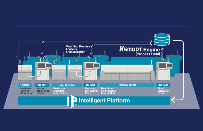
Die Nutzung der 3D-Mess- und Prozessdaten bringt die Produktionssteuerung auf die nächste Stufe. Echte 3D-Messung ermöglicht KI-basierte Prozessmodellierung zur Vorhersage von Parameteränderungen und -defekten oder zur Ursachenanalyse bis hin zu einzelnen Werkzeugen und Best…
Teilen:


