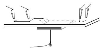
Design for testability (DfT) is obviously a very important issue. The discussion started many years ago with the advent of in-circuit test (ICT) and even denser packed boards. Now it gets even more critical with the use of flying prober board testers, because all of these probes (normally four to XX) need a sufficient landing zone or board pad that has to be provided by the designer during PCB layout considerations.
David A. Sigillo,GenRad, USA; and Luca Corli, Seica s.r.l. in Strambino (TO), Italy
For this work, the designer needs some assistance: mechanical design guidelines for printed circuit boards to be verified with flying probers; and electrical design guidelines for effectively utilizing flying probers in test and inspection. In recent years, with advances in flying prober technology, there has been resurgence in this tester market. Engineering labs, contract manufacturers and prototype or small series shops have been using this technology to debug their assemblies quicker, enabling them to decrease time-to-market. Here we will explore the mechanical and electrical considerations that should be given in any testability analysis to help ensure a successful transition into the prototype and low or medium volume production environment, respectively.
Unlike the in-circuit test (ICT) fixture, the flying prober exhibits mechanical devices that position probes automatically over test targets. Multiple probes are used in these flying probers. There are mechanical constraints that must be adhered to, in order to ensure successful probing. Component sizes, bottom side or top side mounted, test target size, and target type all play a pivotal role in the ability to provide test coverage on the unit under test (UUT).
Electrical debug and test can be greatly improved by following some specific rules for flying prober testing. The location of points for power-up testing, and maintaining specific component pin assignments for capacitors, transistors, diodes, and zener diodes will help in this endeavor. With the use of these guidelines and suggestions, you will be able to move from prototype directly to low-volume testing.
What is aflying prober?
A flying prober is a fast measurement system consisting of tester electronics and an electro-mechanical test head. The tester electronics usually consist of a manufacturing defect analyzer (MDA), or in-circuit test system, in which the test head consists of the roving probe head assemblies that contact the UUT. Modern probers have functional capability such as boundary scan, digital capability and the ability to provide visual inspection. Probers can be integrated into production lines, and are fully configured to Surface Mount Equipment and Manufacturers Association (SMEMA) interface standard. This allows the user to utilize the capital equipment in early production lines, and it provides optimal time to estimate future capital equipment needs.
The benefits of flying probers
The main advantages of using a prober are to speed up time-to-market, improved test access, and cost minimization. These are achieved by the fact that this equipment requires no custom fixture or mechanical adapters to interface to the UUT. The typical turn-around time on a complex ICT fixture is on the order of 1 to 3 weeks, pending board complexity. In some cases, due to time-to-market constraints, fixtures are ordered early, with the understanding that there will be the need to send the fixture back to the vendor for engineering change order (ECO) modifications. This is both costly and inefficient.
The prober is an ideal candidate for low and medium volume production runs. Typically high mix and low or medium volume runs are selected for use with a prober system. Pilot production shops and prototype lines are considered locations where probers can be found.
ICT versus analog only test
Speaking about testing electrical features, the main differences between a traditional bed-of-nails in-circuit tester and a flying prober can be found in the following environments: short circuits test, and integrated circuit (IC) digital test. Both are due to the fact that the flying probers have the access to the UUT with a limited number of probes (typically most manufacturers use four probes).
If a prober is not a very simple MDA, as the first generation was, but they can generate multiple analog guardings and power up the UUT. All the analog components can be measured with a prober as it is similarly done using a bed-of-nails tester. Only the testing time will differ for the user. This testing time, depending upon the prober and the UUT tech-nology, should be from 3 to 7-times greater. A user can accept this time increase to have the same electrical per-formances of a traditional in-circuit tester.But this is not true for the shorts test. Ifa UUT has N electrical nodes, the possi-ble total shorts (TS) between two nodes are:
TS = N(N-1)/2
In a bed-of-nails tester, all the possible total shorts (TS) are normally checked, even if most of them have a very low probability to exist, since the possibility to have access to all the nodes at the same time allows to do the job in a very short time. For example, if N=500, a bed-of-nails tester needs M=N=500 measurements to detect the shorts, because each node is tested against all the others at the same time. However, a flying prober checking each possible pair of nodes needs:
M = 500(500-1)/2 = 124,750
This very high count of measurements is necessary to do the same in the worst case. Or, assuming checking one node against three others each time:
M = 3p(p+1)/2 + q(p+1) = 41,750
Where is the best case:
p= int((N-1)/3)
d= (N-1)/3 –p
If d=0 === > q=0
If d=0.3 === > q=1
If d=0.6 === > q=2
It is clear that a flying prober needs a software algorithm to reduce the number of shorts test, because the bed-of-nails method is not applicable due to the dramatic test time increase. For that goal, some probers are equipped with software tools, analyzing the geometry of the PCB (Gerber files), to exclude from shorts test the measurements on the nodes pairs where it is not probable to find a short circuit (caused mainly by the manufacturing process). The software is typically looking for a minimum clearance between pads, pins, vias or tracks, to decide if two nodes can be shorted or not. The total amount of the shorts measurements can be reduced to up to 1% of the total possible shorts (TS), by maintaining the shorts fault coverage above 99%, assuming that the UUT is new. This is because board assemblies coming from the manufacturing process (not from the field) typically have high reliability of the electronic components.
On the probers equipped with extra-fixed channels, the remaining testing time for shorts can be reduced again, by placing some fixed probes on the opposite test side on the power and ground nets, or by using a cable wiring a UUT edge connector with the tester.
Concerning the IC digital test, it’s obvious that four moving probes perform a truth table check for simple logic gates only. On the other hand, the increasing complexity of the digital components (increased number of package pins), and their high reliability, is moving the need of the user from component testing to process verification. For that reason, normally it is not strategic to test the functionality of a digital component. Therefore, the user is not concerned if a flying prober is unable to do that, since it is much more important to check that the digital component is mounted and soldered correctly.
It is also true that a flying prober equipped with power supplies and digital capabilities (via moving and fixed probes) can help the user in the test program fault coverage maximization, by performing the following additional test methods:
• Analog IC tests (op-amps, AD/DA converters, etc.)
• In-circuit (P/PLD/memory devices programming (by serial protocols)
• Boundary-scan test
• Logic signature analysis
Test pad and pitch requirements
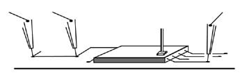
Generally speaking, the larger the test pads the better the probing. As with standard in-circuit fixturing, the PCB designer should strive to keep the test pads as large as possible. The typical test pad size for probers is 10-mil. Some prober manufacturer claim to be able to probe 4-mil pads. For small surface mount devices it is sometimes best to elongate the land where the lead or bump is mounted so that it can be probed. Software algorithms, also known as pad nudge routines, which automatically position the prober pin adjacent to the soldered lead, accomplish this.
The typical pitch requirement between test points is 16-mil. In most cases, even tighter pitch tolerances down to 12-mil can be achieved with some success using fine-pitch probes. With 16-mil pitch, the maximum test pad size of the two adjacent test points in question could be approximately 12-mil.
Z-height requirements
While test pad and pitch requirements are rather consistent from vendor to vendor, the z-height requirements can differ. This prerequisite is the prober’s limitation to probe UUTs with tall components, for example, heat sinks, connectors, board mounted transformers, etc. Pending the prober chosen, different test equipment vendors have different approaches to mounting the axes that carry the probe, and as a result, transverse over these tall components. In some cases, the UUT has significant tall components that limit the travel of the support probe structure over the UUT. There are three main approaches chosen by the vendors to avoid these limitations: no-fly zone; probes top mounted on surface linear motors; and probe supporting structures designed sufficiently high enough.
The use of no-fly zones enables the probe and its accompanying axis structure to ‘
move over the UUT and avoid the tall components. Taking the CAD data and graphically depicting or highlighting the tall components during the test program development usually accomplishes this. By running this data through proprietary software, the probe structure and axis will essentially avoid the areas with tall components.
Another alternative is the use of top mounted surface linear motors. These motors are mounted well above the UUT, and typically have far greater z-axis capability. One disadvantage of this approach is that the surface mount motor plate typically impedes the user from viewing the UUT.
The most common approach is to design-in sufficient clearance for all possible maximum height components. If this cannot be achieved, or if a UUT has been introduced which exceeds the z-height specification of the prober, then the no-fly zone method can be used to achieve the same result.
Board positioning requirements
It is very important to have board fiducials or markers added to the UUT during the development phase of the board. These markers are used extensively in the board set up prior to testing. The approach used by most vendors is to align the probes to the UUT by visually inspecting the location of a fiducial. Once the center of the fiducial is determined, an offset (the delta distance between the vision center of the fiducial and the theoretical center based on CAD data) is added to the X and Y locations of all the test points. After this is achieved, the test may commence.
The board markers are used in manual and automated mode. In manual mode, the boards are installed in a specific location against a mechanical board stop or tool pin. The camera inspects for the board fiducial, calculates offsets and the test is started. In automated mode, the board is presented to the prober, and once it is cleared via the appropriate SMEMA signal, the board is transferred to the prober test head. Here again, the fiducials arelocated, offset calculated and testing started.
Automationrequirements
Like most other typical in-circuit and functional testers, the probers can be set up to operate in an automated line. The probers must follow the SMEMA interface standard to operate properly. The input and output shuttle or loader must meet the height restrictions for the SMEMA line, which is adjustable from 37.0 to 38.0-in from the plant floor to the bottom side of the UUT.
The signals may be obtained by using an optical isolator or a relay. The minimum requirement is to switch 30V at 10mA. At 10mA, the output “low” must not exceed 0.8V. The logic is as follows:
• Board transfer occurs when machine A has a board available (contact closed), and machine B is not busy (contact closed)
• The signals can occur at anytime, but board transfer does not occur until both contacts are closed
• The board-available signal from machine A will remain closed until the board has left machine A
• The ready signal will remain closed until the board has arrived at machine B
• Board transfer cannot occur again until each signal opens for at least 50ms
• Optional: Once both machine A and B signals are closed, and the board has neither left A nor arrived at B, an error message will be generated.
Vision systems
Vision systems have been successfully integrated into probers to augment electrical test. Generally, the following vision inspections can be done by various integrated systems: absence and presence, multiple object testing, image recognition, and component orientation. A key factor in utilizing vision inspection is to be aware of strengths and weaknesses. Utilizing vision is basically a “learned” process. The user must use a known-good board (or golden board) and learn the parameters of the board that is to be inspected with vision. The latest vision software packages have made significant improvements in this aim.
Summary of mechanical design guidelines:
• Via holes need a minimum diameter of 12-mil, and must be free of solder resist
• Whenever possible, via holes should be filled and free of solder resist
• For SMDs, especially for those with less than 25-mil pitch, the solder pads should be elongated so that the probe can contact the pad and not the lead
• Components taller than 20mm should be positioned on the opposite side of the test side if the board is double sided
• Components taller than 20mm should be placed as far as possible from the center of the board if the board is single sided
• Components should not be closer than 2mm from the edge of the board. This will ensure that the board can be retained properly
• When using open capacitive probing techniques, ensure that all ICs are on the same side of the board
• Perform testing on the board prior to installing components or mechanical mounting structures which would prohibit probing
• Provide two or more board markers/fiducials for positioning on the diagonal. The markers should be round and free of tin, solder resist, or overspray
• In multiple boards (panels), provide markers on every board in that panel
• A recommended tooling pin size of .156-in (+.003/-.000) located on the front edge of the UUT
• Tooling pins should be located .300-in (±0.01-in) from the edge of the UUT
Electrical test points
Here, test point means access to an electrical node for the probes of the tester. A test point can be a test pad, a via, a through-hole component pad, an SMT component pad, or a component leg.
The new generation of flying probers, working as traditional in-circuit tester with guarding capabilities, needs at least one electrical test point for each node (net), positioned on the same side of the UUT, in order to become a virtual bed-of-nails tester. It is not necessary to probe always on the legs of the component, since this is not a good idea for open checking. To improve the test speed, some probers can accept and use more than one test point per net. The management software can decide which test point should be used for the next measurement, depending on the positions of the previous probes.
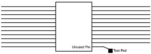
It is also very important to provide test points for unused pins. In fact, a short circuit between one unused and one used pin can create a lot of problems in the UUT’s real life, but the prober cannot detect it if the access to the unused pin is missing. On the other hand, a flying prober has fewer problems than a bed-of-nails tester in this case, because often it can probe directly on the components legs (allowed for shorts test), if the components are mounted on the probed UUT side.
On the opposite probed UUT side, a smart designer can provide one big test pad (100-mil diameter) for each power and ground net. These pads will be used to connect fixed probes (on equipment equipped with that feature) to power up the board, but also for adding guard points and reducing test time.
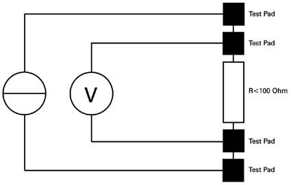
In order to perform Kelvin measurements on small resistors, typically lower than 100h, the designers should provide two test points for each net related to those components. In this way the residuals of the system will not affect the resistance measurement.
All the test pads should be numbered in the CAD system. The number can be used like a virtual channel number in the test program, and if it is printed, also in the schematic drawings. It will also help the manual debugging process. Again, if the test pad number is printed directly on the PCB (where possible), the physical manual test point adding/modifying will be easier, without referencing a paper document.
Decoupling components
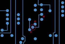
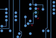
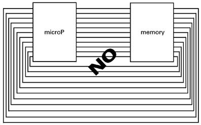
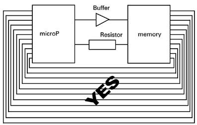
The main goal of the in-circuit test is to check the UUT by performing many single measurements on all components one by one, even if they are connected since they are already mounted on the PCB. To allow this, each component must be electrically isolated from the rest of the UUT and all others must be disabled. The designers should avoid connecting two digital components completely in parallel, as shown in the figure.
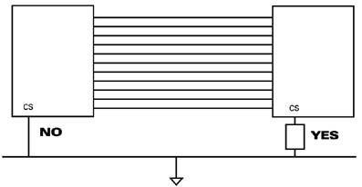
A simple resistor (typical value 330h or a buffer can solve the problem. Electrically nothing changes in the UUT functionality, but each component can be fully tested, since all the inputs are independent of the outputs of the component previously connected. Also, when two or more digital components are connected to a bus, the designers should avoid tiring chip select and/or enabling pins directly to GND or VCC. By inserting a small resistor (typical value 68h for TTL or 220h for CMOS logic), it is possible to enable/disable the component when another one on the bus must be tested.
A completely different problem can be easily fixed again by inserting a decoupling component. When a battery or a super capacitor (0.1 to 1F) is mounted on the UUT, the short test or other low voltage analog measurements can be very difficult, because of the „high” source voltage that power up the board or one of its sections. By providing a jumper to isolate the battery or the supercap during the test, the designer can avoid this inconvenience.
Components/netsnames and labels
Some simple rules to follow in the writing of CAD files can also improve the automatic test program generation for the UUT. For example, it is typically helpful to give different label names to different component types. Dxx for diodes, LDxx for LEDs, DZxx for zeners instead of a generic Dxx for all components, or Cxx for normal capacitors and CPxx for polarized capacitors. Also, Rxx for resistors, RPxx for resistor packs and RTxx for trimmers etc. By following these simple rules, the automatic test program generator software can optimize the program from the beginning, by reducing the manual work of the user.
A common error that some designers make is to assign a generic name like unused or “nc” to all ICs not used in the UUT. This will create a lot of problems in the short tests, because all these pins are considered shorted together, connected to the same node. So, even if no test pads are provided for unused pins, a flying prober can contact directly on the components legs. The designer must assign a different net name to them. This will allow a correct short circuits automatic test program generation.
Miscellaneous
To increase the speed of testing, a simple connector carrying the power and ground nets can be provided on the UUT for test applications. In this way, some extra-fixed channels can be connected to the UUT, to increase the number of guarding points. Of course, it will be possible to easily power up the board by avoiding use of the fixed probes on the opposite probed side. The same method should be used when boundary-scan components are mounted on the UUT. A connector carrying out the TDI, TMS, TCK, TDO and TRST (when present) signals will be very helpful toperform boundary-scan test via fixeddigital channels available in the testing area.
If some heat-sinks are provided for SMT ICs, those should be mounted after testing, to allow the opens check by using vectorless methods based on extra probes positioned on the component packages. In fact, this kind of measurement, executed by a moving or a fixed extra probe, needs to contact the case of the component, to sense an AC signal. This will be impossible if the package surface is not free.
To respect high quality procedures for testing, a simple method can be used to understand if a UUT was already tested or not. The designer can provide a thin track on the PCB, connecting two test pads,and this will be burned electrically by the tester at the end of the test program (the prober must be equipped with instruments to supply high currents, typically 5 to 6A). When a bed-of-nails test is available, many users do the same job by using ink stamps provided in the test fixture, which is obviously impossible by using a flying prober.
Electrical design guidelines
By resuming the electrical design guidelines, they can be assigned to the three different categories such as mandatory, recommended and suggested.
Mandatory:
• At least one test point for each electrical node of the PCB
• A different net name for each unused pin of ICs
• Decoupling resistors for chip-select/enable pins of digital ICs
• Big test points on the opposite test side for powers and grounds
• Different label names for different component types
• Avoid connecting two or more ICs completely in parallel
• Decoupling jumpers for batteries or supercaps
Recommended:
• Two test points for each net related to resistors (100h
• One test point for each unused pin of ICs
• Assign test pad numbers in CAD design
• Print test point numbers in schematic drawings
• ICs heat-sink mounting after testing
Suggested:
• Print test pad numbers on the PCB
• Test connector for power and ground
• „Fuse-track” for test quality certifying
These mechanical and electrical guidelines can be used successfully to efficiently apply the moving probe equipment. The flying prober is clearly a very valuable tool when used properly in the right production environment.
David A. Sigillo, BSME, bachelor of science in mechanical engineering, University of Massachusetts, Amherst, and masters in management science and manufacturing engineering, University of Massachusetts, Lowel, is a business development director at GenRad, Inc., in Westford, Massachusetts. Previously, he was the project leader for test systems, and custom engineering manager.
Luca Corli holds a BSEE from Politecnico di Torino, Italy. He is the sales support manager at Seica s.r.l. in Strambino (TO), Italy, and he was involved in field application engineering for in-circuit and functional test systems.
Zusammenfassung
Schon immer war der Schaltungsentwurf, der die Testbarkeit zu berücksichtigen hatte (Design for Testability) eine große Herausforderung. Mit der Anwendung der Flying-Probe-Tester aber ist beim PCB-Design noch mehr Nachdruck zu verspüren, müssen doch die Prüfnadeln ausreichende und sichere Kontakte auf den Boards finden, um optimal zu funktionieren. Layout-Betrachtungen aus der Sicht des Prüffelds sind also unumgänglich.
Résumé
La conception de circuits, devant tenir compte de l’aptitude aux tests (design for testability), a toujours constitué un enjeu important. Avec l’application des testeurs d’échantillons « flying », la conception des PCB (cartes à circuits imprimés) est confrontée à d’autres difficultés car les broches de contrôle doivent trouver sur les cartes suffisamment de contacts fiables pour pouvoir fonctionner de façon optimale. Les observations d’implantation au niveau du champ de contrôle sont par conséquent indispensables.
Sommario
Da sempre la progettazione di circuiti rappresenta una vera e propria sfida, soprattutto làddove sia necessario tenere in considerazione la controllabilità (design for testability). Con l‘utilizzo dei Flying-Probe-Tester si nota nel design PCB uno sforzo ancor maggiore, in quanto gli aghi di controllo devono trovare sulla scheda dei contatti sufficienti e sicuri, al fine di poter funzionare in maniera ottimale. Osservazioni del layout dal punto di vista del settore di controllo sono dunque inevitabili.
Fax +49-89-96285-101
EPP 188
Unsere Webinar-Empfehlung
Die Nutzung der 3D-Mess- und Prozessdaten bringt die Produktionssteuerung auf die nächste Stufe. Echte 3D-Messung ermöglicht KI-basierte Prozessmodellierung zur Vorhersage von Parameteränderungen und -defekten oder zur Ursachenanalyse bis hin zu einzelnen Werkzeugen und Best…
Teilen:


