Sophisticated technology, different types of package and, of course, the ever-reducing size of structures are main factors that require an innovative approach for effective optical test equipment. A multitude of tasks in demanding surface inspection can now be addressed with a versatile measurement system.
Dr. Gisela Dittmar, in charge of UBM Messtechnik, Germany
A system of UBM Messtechnik reduces the overall investment without compromising flexibility and test capability. Whether such a system is used as a pure QA tool or for R&D applications, the versatile, exact and easy-to-use instrument helps in the development and optimization of procedures and in the monitoring of manufacture.
The knowledge of the geometrical properties of the surfaces and fine structures on devices, wafers, chips, PCBs, encapsulations and leadframes simplifies the control of modern manufacturing processes. It allows manufacturers to alter parameters during the process to improve the production and subsequently optimize the yield. The use of non-contact measurement techniques is highly advantageous when considering extremely touch-sensitive layers, such as fresh screen print structures made from conductive, insulation or solder pastes.
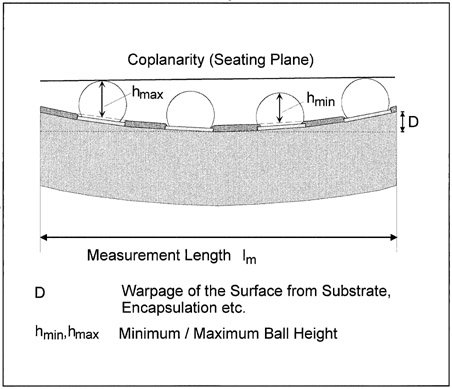
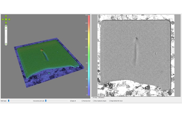
Along with characterising lateral dimensions along the XY plane, the determination of the height parameters in the Z direction is important too: structure or step heights; depth of structures, coplanarity of pins; board or substrate warpage and surface roughness.
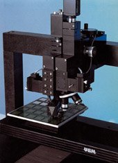
To address these parameters, the company has developed an instrument to closely match the demands of advanced manufacturing. The instrument comprises many functional units such as laser-optic sensor, precision measurement stand with motorised XY translation stages (with air bearings if desired), process control unit, microscope and optional video camera for initial set-up and real-time observation of the measurement area, workstation and the appropriate software. For special applications such as inspection of BGA or wafers bumps, an optional image processing system is also to incorporate.
With a range of motorized translation stages, the measurement length in XY directions can be set between 0 and 300mm. This allows measurements to be defined at different positions on a particular package or at different positions on a number of packages, and nearly all package types can be accommodated. With lateral resolutions in the XY plane of approximately 1µm and a positioning accuracy of approximately ±0.5µm, the system is ideally suited for high requirements. In the Z direction there is a maximum measurement range of 1mm and this is coupled with a maximum resolution of 0.006µm.
The software provides automated and freely programmable measuring procedures, statistical evaluation, task administration, trend analysis (optional SPC module) and 2-D and 3-D graphic display of the results on either monitor or printer. Manual measurements and analysis may also be performed if required. Utilising a combination of the analysis features incorporated, this system simplifies the task of quantifying measurements and more importantly, devices under test can be quickly identified and eventually fixed.
Warpage within limits
The determination of warpage is important for a number of steps during the manufacturing process. Should the warpage exceed a certain value then the possibility of fixing a ceramic substrate or PCB onto the vacuum chuck of a printing table or wire bonder becomes impossible. In addition chips either do not attach properly or even delaminate from too warped leadframes, encapsulation bottoms, ceramic or PCB materials, MCM boards, BGA or flip chip assemblies. If the substrate itself is too warped, then it is impossible to get a satisfactory contact during BGA or flip chip assembly. Where packages are laser marked there is also an increased risk of damaging the bonding wires if the plastic encapsulation is warped too much and is too thin after the moulding.
In thick-film screen printing or adhesive and solder paste printing, warpage has a great influence on the result. The significance of the photolithographic process in the manufacture of MCMs is increasing as structures continue to get finer. This is particularly true in multichip technology, so the control of the process is critical. Here the requirements placed on the measurement equipment are almost reaching those which apply to wafer processing.
Controlling roughness
Determination of roughness parameters is also of great significance for many processes. For example, the wire bonding may be significantly affected by too high roughness on the bond pads so that the bonds subsequently fail. Other example in which roughness can be critical is in the thick-film technology. Too high roughness greatly alters the performance of a paste mask so it has to be changed or other pastes applied to achieve the desired results. The creep of paste and paint can also be affected and as a result components may require rework – this is expensive and typically leads to a decrease in yield. On the other hand, too low roughness can lead to low-quality die bonding with adhesives for component assembly.
Integrated circuits are manufactured by the deposition or removal of layers with simultaneous or subsequent structuring. To monitor that processes for optimization or further development, the height, width and depth of these structures must be accurately measured.
For setting up screen printing parameters and selecting suitable masks, it is necessary that the heights of the layers and the width of the structures are measured and that both the surface profile and shape of the structures are recorded. During production it is important to regularly measure the height or the volume of the paste. Applying too much solder paste can lead to shorts and is wasteful, too little can lead to insufficient joints. Furthermore, when changing batches or paste types, repeated printing tests followed by measurements are recommended to establish the appropriate printing parameters before actual production is recommenced.
The possibility of determining thickness by measuring on wet layers has the advantage that faulty PCBs or components may be cleaned and reused so waste is reduced. However, most important is that by measuring the wet layers shortly after printing, alterations can be quickly made to the process so expensive rework following placement, soldering or curing can be minimised and costs considerably reduced.
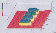
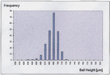
When developing new package types, many parameters must be measured. For instance, to ensure the correct assembly of BGAs or flip chips, the heights of the bumps should be within a certain tolerance. For this reason measurement of the bump heights and the warpage of the substrate is imperative. For this application, the instrument also incorporates image processing capability to determine presence, diameter and position of the bump’s center, and in addition to this the heights of the contact points are measured by a laser-optic sensor. Unique to the system for BGA measurement, as well as measurement of the coplanarity, the absolute bump height is also calculated taking the substrate warpage into account. This factor is often overlooked but is critical to the performance of the assembled package.
Height and profile measurement
Considering wire bonding, it is important to make sure that the heights of bond pads, the thickness of chips and the height or coplanarity of the leadframes´ inner leads are within tolerance. Failure to ensure such parameters fall within acceptable limits will inevitably lead to increased failure rates and rework costs.
UBMs measurement system provides an advantage over other inspection equipment by combining both laser-profilometry and image processing. Due to the high lateral and vertical resolutions, even sophisticated parameters can be quickly and easily determined using a single instrument. With automated measurement and analysis procedures the system can be easily integrated into the production floor. Coupled with a large range of measurement capabilities the investment pays back soon.
Fax +49-7243-517-111
Email: UBM@compuserve.com
EPP 209
Die optische Vermessung von BGAs oder Flip-Chips und Substraten wird zunehmend anspruchsvoller. Um zahlreiche anspruchsvolle Inspektionsaufgaben an mikrostrukturierten Oberflächen durchzuführen, bedarf es jetzt nur noch eines Instruments, das vielseitig erweiterbar ist und damit hilft, Prozesse zu optimieren und Kosten zu begrenzen.
Le mesurage optique des BGA ou Flip-Chips et substrats devient de plus en plus exigeant. Pour pouvoir réaliser de nombreuses opérations d’inspection sur des surfaces microstructurées, il ne suffit maintenant plus que d’un instrument susceptible d’évoluer et donc de contribuer à optimiser les processus et à limiter les coûts.
La misurazione ottica di chips BGA o di Flip-Chips e di sostrati diventa sempre più complessa. Per eseguire numerose complesse operazioni di ispezione su superfici microstrutturate è sufficiente oggi disporre di un unico strumento ampliabile che aiuta a ottimizzare i processi e a risparmiare costi.
Unsere Webinar-Empfehlung
Applikationen aus dem Bereich der Leistungselektronik gewinnen immer mehr an Bedeutung. Die Inspektion dieser Applikation lässt sich mit der bewährten Standardtechnologie der 3D-Messtechnik bewerkstelligen.
Teilen:


