


The rework of board assemblies has never been more critical. Once viewed as either a minor annoyance or as a cost source rather than a revenue generator, the process has been put onto center stage through economical and technological challenges. Maintaining even razor-thin profit margins and good product quality is dependent upon the ability for efficient rework.
Howard Rupprecht, Metcal, UK
Most manufacturers recognize the essential value of rework and repair. However, even with this understanding, many engineers and shop floor managers retain an “old style” mentality when it comes to establishing the procedures and organizing the tools needed for cost-efficient rework. When setting up an SMT production facility, a high-volume manufacturer employs a team to research, source and develop the process. It spends months investigating equipment and materials, and more time is used installing machines and implementing the process. Stringent quality control measures are initiated to guarantee accuracy and repeatability.
Having learned the important lessons about soldering and placement when setting up the SMT line, well-meaning engineers will often disregard these very same factors when it comes to repair. A simple rework unit and a few hand tools are expected to perform the same functions as a complete line – and do so with the same degree of repeatability and accuracy. Board value and therefore financial risk is highest at the research stage as the board is not fully assembled and the value added.
As rework has grown in importance, the tools and procedures become increasingly critical. A well-run repair department requires solder/desoldering units, soldering irons, tips, hand tools, paste application and cleaning equipment, inspection tools, workbenches and fume extraction systems. There must also be adequate lighting, storage space and anti-static accessories.
1. The basic steps
With the advent of SMT, fine-pitch devices, BGAs, CSPs and array packages of all types, the steps have evolved, and decisions made along the way are not as evident as they once might have been. Yet the basic step-by-step process remains essentially the same:
• Identification/problem analysis
• Component removal
• Surface preparation
• Component replacement
• Final inspection
2. Identifying the problem
The first task is to establish the severity and nature of the problem: is it a failed component, improper alignment, a solder failure, or a poorly fabricated PCB? The answer will determine if the task at hand is to simply touch up a pad, or if a particular component must be reflowed, realigned or replaced. This first step is obvious, but the types of components that can be involved complicate the matter.
The next decisions are dependent upon type and cost of component, board cost, time and technician skill: removing the device with convection or conduction? Once the problem has been identified, the technician must make another basic evaluation: will the desoldering method be conduction (soldering iron and tips) or convection (hot air)?
3. Conduction soldering: pros and cons
The conduction approach is well understood and has been part of the industry almost from the outset. Using a soldering iron and matched tip (to component size, shape, and temperature range), the solder joint is physically touched and heated. To touch a lead with the soldering iron tip, the lead itself must be visible. It follows that only QFPs, PLCCs, and various discrete components are candidates for conduction. For array packages, convection alone is the method.
Conduction has its advantages: cost for one. The equipment, including a soldering iron and tips, is inexpensive. The process is easy to learn: select a tip best suited for the particular component, and simply use the iron to reflow the solder so that the device can be removed. Because direct heat is used to melt the solder, conduction is the fastest method of removing components.
Conduction does, however, have several disadvantages. Primarily, the success of conduction depends on the skill of the technician. Just as the process can quickly reflow solder, it can just as quickly damage the component or the PCB itself. If the operator holds the tip on the joint too long or uses a wrong iron and tip, the PCB can be irreparably damaged and pads can be lifted.
It seems useful to highlight some points about performance of the conduction method. First, tin-lead solder melts at 183°C. The basic rule of thumb when using a soldering iron is to use the most minimum temperature possible – a tip temperature that will allow reflow in reasonable time but poses minimum damage to the PCB.
Some soldering irons work on the “fixed power, variable tip temperature” principle. As this implies, power (Watt) is constant and the operator, using a dial on the control unit, adjusts tip temperature. But a single fixed power is often too much for a light solder joint and not enough for a heavy one. And because temperature settings can be changed from day to day, job-to-job, operator-to-operator, results may be inconsistent. To further complicate matters, those units must be constantly calibrated to ensure that a tip is indeed reaching and not exceeding its temperature.
Metcal has developed SmartHeat – a variable power, fixed tip temperature that allows for conduction at minimum controlled temperatures. With this system, the metallurgical qualities of the tip determine temperature. The self-regulating tip (Curie-point principle) automatically adjusts power to maintain constant temperature – eliminating many of the problems that are seen with fixed power units. SmartHeat maintains an accuracy of ±1.2K. Because the operator can’t adjust it, process repeatability and consistency are greatly improved.
Even in the case of leaded components and discretes, the choice of conduction may not be straightforward, because its reusability is a primary concern. If a removed com-ponent is faulty, conduction makes sense, as the device will be scrapped. On the other hand, if 200 high-value compo-nents have been placed automatically the wrong way around, it is economical to reuse them. In fact, the ultimate scrap-or-rework decision is very often dictated by the reusability of components. The conduction method can leave perfectly good components with damaged leads and excess solder on the leads. Reusing such a component may be a problem and will need additional clean up – which, in turn, requires more time spent and higher overall rework costs.
4. Convection soldering: pros and cons
Because convection offers much greater process control, it is the preferred method when component reusability is an issue. This is true for array packages, expensive military/aerospace boards, and tightly packed or critical assemblies that require optimum reliability. Convection provides a more controlled method of desoldering. Depending upon the sophistication of the rework system (manual or semi-automatic), convection can offer precise temperature control, component profiling, split-beam prism alignment systems for array packages, and more.
There are two basic types of convection systems – those using high and those using low air flow. The latter are preferred, because they el-iminate the problem of adjacent components. When heating a component using hot air convection, adjacent devices may reflow. This can become a problem when the hot air begins to move adjacent components out of alignment. With low airflow systems, adjacent devices are not disrupted.
5. Assembly factors
With both conduction and convection, board weight, material, and layout will influence temperature consideration and, in the case of conduction, tip temperature-range selection. Operators must avoid high temperatures when dealing with delicate materials and sensitive components. Conversely, heavy ground planes draw heat off the joint, and a higher energy is required to bring the joint up to solder melt temperature in a reasonable time. Densely populated boards require finer tips for access (using conduction), and limited air flow (for convection) to avoid damaging adjacents. Both processes require a higher starting temperature to achieve faster heat transfer to the joint.
6. Pad preparation
Having removed the component, the next step is to check pad integrity and the quality of the solder. If it is possible to use the existing solder, it is important to remember that the crystal structure of solder will change as it is heated and reheated. In cases of critical rework, where the highest quality is demanded, it is best to remove the existing solder and start the process again. Starting from scratch, so to speak, is the only option for array packages – in general, when removing the device (using convection) about 50% of the solder will also be removed.
For leaded and passive devices, it is possible to use the existing solder. With a soldering iron and a hoof-type tip (that holds an amount of solder), the tip can be pulled across the range of pads, and solder is deposited. The process is time-consuming and requires some skill, but it is an inexpensive alternative removing residual solder, cleaning pads, reapplying solder paste, etc.
If solder is to be removed, technicians will generally use a precise temperature-controlled desoldering tool. Once the site is clean and the pads are clear of solder, a measured amount of solder paste can then be applied to the pads. For many, the preferred method of removing residual solder is with desoldering braid which can be fast, safe, efficient and economical. Using braid is not difficult, although it does require skill. The operator will contact the solder to be removed with the iron and the braid, paying careful attention keeping the wick between the tip and the board itself. Direct contact of the tip to the board may result in damage.
If the particular process requires that the area be cleaned before reapplying solder, it is important to follow the parameters established for that specific board. Solvents should not be allowed to migrate onto surrounding pads as their no-clean characteristics may become compromised.
7. Replacement and resoldering
When re-working with discrete components, device removal can be accomplished using heated tweezers or a soldering iron. The component is then replaced by manually resoldering onto the PCB, normally with the use of solder wire. The tip must be carefully chosen to match the pitch of the component, and it must not touch the substrate.
With finer leaded QFPs, the conduction method is viable – but not if the ICs will be reused – as there will be a substantial amount of solder remaining on the pins and the pads. Solder braid can be used to help remove excess solder from the pads. Alternatively, a hoof tip can be used to reflow the solder into a degree of uniformity. A reused IC can then be put on the pads, tacked on two corners to hold it in place, and then flux can be applied, and solder can be dragged to the leads and the pads. Another method for working with QFPs includes the use of solder paste and the convection method. Using a hand-held hot air tool, for example, the IC can be removed. Pads are then cleaned and solder paste dispensed onto them. The IC is replaced, and the convection tool is used to reflow the paste.
With standard-pitch ICs, paste can be applied as beads, and during heating they will most likely flow to the wetted leads. The results will be good but not perfect – and a few solder shorts may need to be touched up. With fine-pitch ICs, a mini-stencil is needed to apply the paste. Depending upon the level of process control required, a hand-held convection tool can be used with certain array packages. However, the PCB could be damaged in the process – as there is no temperature profiling – and the replacement of the BGA, for example, would be hit-and-miss at best.
8. Special case: fliped chip replacement
Rework with BGAs and other flipped chip packages demands a high level of process control. There may be 1,000 terminations beneath such an IC, and only one incorrect solder joint could require a second round of replacement. The goal is to get the process right the first time. The requirement for temperature control is much higher than for conventional SMDs. With BGAs, one must heat gradually through the package to reflow the solder connections. If temperature, ramp and dwell time (2 to 3K/s) are not strictly controlled, simultaneous reflow will not occur and a damaged part is likely. Establishing a consistent thermal profile for BGA removal is tricky. Information on each package is not always available, and the hit-and-miss method may cause thermal damage to the substrate and surrounding components or lifted pads.
There are hot-air rework systems that make BGA removal and replacement relatively easy. Generally, the air is forced through a nozzle at the temperature (determined by the thermal profile) that will reflow the solder but not damage the substrate or the surrounding components. The type of nozzle varies with equipment and with operator preference. Some systems flow air above and below the BGA, while others move air horizontally and some to the top of the device only. Some prefer a shrouded nozzle that protects surrounding components by focusing the hot air directly onto the component. During BGA removal, dwell times are critical. The key is to pre-heat the underside of the PCB to prevent warpage. BGA replacement, because it requires a multi-zone reflow process, demands accurate process control and patience. Moreover, rework with BGAs is definitely slower than with other SMD, in the order of 8 to 10 minutes per component.
9. Inspection
Positional accuracy, cleanliness, joint formation, wetting, bridging and sufficient solder are all parameters that need to be inspected. With leaded components, it’s simple to look for the solder joints. A low-magnification inspection tool can be used for passive and standard-pitch devices. When inspecting around 25-mil pitch and finer, the magnification and image capabilities of the system need to be much higher to accurately see the quality of solder and joints. Of course, any manual inspection is open to individual interpretation by the operator. With flipped array packages, the best inspection method employs X-ray to see underneath the components. Yet, even expensive R-ray inspection cannot guarantee an accurate view of all joints.
10. Added-value consideration
As assemblies become increasingly expensive and profit margins remain thin, rework is becoming more complex and all the more critical to bottom-line profitability. To add value to total manufacturing, rework must be both cost-effective and meet quality and performance standards. To achieve these goals requires thorough operator training and hands-on experience, coupled with the proper tools needed to work with the full range of component types – from through-hole to standard SMDs, BGA, CSP, flip chip and beyond.
It was once possible, perhaps even economically feasible, to limit rework ( to accept high scrap rates and pay little attention to the process. However, ignoring rework or allowing untrained operators to use outdated tools is no longer a wise course of action. The result of such a short-sighted approach can be economically perilous.
zusammenfassung
Die Nacharbeit von Baugruppen war relativ leicht mit konventionell-bedrahteten Komponenten, doch hochintegrierte und dichtgepackte SMT-Boards sind kritischer denn je im Reparaturbetrieb zu löten. Hinzu kommen die geflippten bzw. Area-Array-Packages (BGA, Flip-Chip, CSP usw.), bei denen sehr hohe Präzisionsanforderungen sowie die Versorgung der Anschlüsse mit Fluxer und Lotpaste sowie das Durchfahren eines exakt spezifizierten Temperaraturprofils den Austausch noch verkompliziert.
Résumé
La retouche de modules était auparavant une opération relativement aisée avec des composants à connexions classiques. Or, les cartes SMT (surface mounting technology) à hautes intégration et densité sont de plus en plus difficiles à braser dans le cadre de réparations. Par ailleurs, les «area-array-packages» et les «flipped packages» (BGA, flip-chip, CSP, etc.), lesquels demandent une très grande précision ainsi que l’alimentation des raccordements avec poste de fluxage et pâte à braser et le profil de température précis, compliquent encore plus le remplacement.
Sommario
La postlavorazione di gruppi costruttivi con componenti a cablaggio convenzionale era relativamente semplice, ma la brasatura per la riparazione di schede SMT ad alta integrazione e ad alta densità è molto critica. Ad esse si aggiungono i Packages flippati o gli Area-Array-Packages (BGA, Flip-Chip, CSP etc.), nei quali gli altissimi requisiti di precisione cosìccome l‘alimentazione dei collegamenti con fluxer e pasta di brasatura o il rispetto di un profilo di temperatura esattamente specificato complicano ancor maggiormente lo scambio.
Fax +44-2380-489-109
EPP 157
Unsere Webinar-Empfehlung
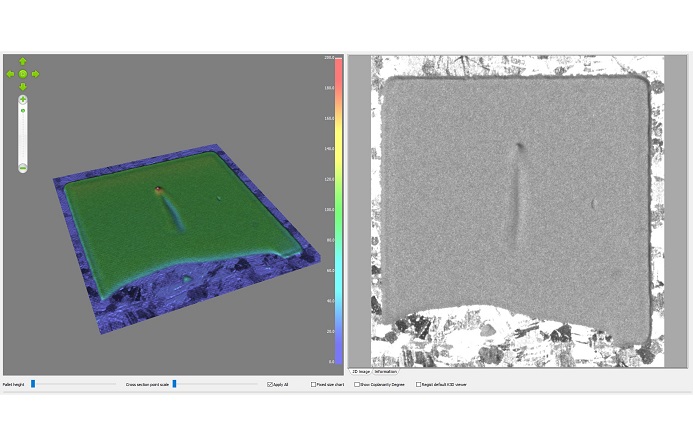
Applikationen aus dem Bereich der Leistungselektronik gewinnen immer mehr an Bedeutung. Die Inspektion dieser Applikation lässt sich mit der bewährten Standardtechnologie der 3D-Messtechnik bewerkstelligen.
Teilen:


