

According to the current roadmap of leading German solar-cell manufacturers, a yearly cost reduction of about 10 % is required in order to keep solar energy competitive beyond the current feed-in-tariffs. For PV generated energy to reach the price levels of conventional energy, the costs along the entire value-chain must be optimized. For the last step in solar cell production, contact metallization, this entails not only cutting costs in the manufacturing operations but also in the production machines themselves.
Asys Group, Dornstadt (Germany)
With a varied offering of high-throughput solutions, Asys has well anticipated these price demands and is thus the ideal choice for cost-optimized metallization lines. With an unmatched throughput of 4600 cells per hour, market leading uptime and low breakage rates, the company ensures optimum efficiency for solar cell production.
Imaginative solutions
Constant pressure to lower costs in the photovoltaic industry demands innovative solutions from the manufacturers. Consequently, to reduce the amount of the expensive raw material used, the solar cells are becoming increasingly thinner. The production machines of the german manufacturer can handle solar cells down to a thickness of 120 µm, which already exceeds the target that many solar manufacturers were aiming to achieve by year 2015. For metallization of solar cells, the role of efficiency enhancing laser technologies is particularly growing in importance. To maintain maximum cell efficiency, the interaction between the laser structuring and metallization processes must be optimized, which can be achieved using vision systems for cell measurement and position recognition. Increasing cell efficiency results in higher power modules and thus greater power concentration in the overall installed PV system. This in turn lowers „Balance of System“ (BoS) costs, since there is considerable amount of installation cost included in the overall system cost. Considering the „BoS“ clearly demonstrates that an increase in solar cell efficiency is by far more effective at lowering cost/Watt than those achieved by reducing the costs of the solar cells or the production machines by themselves. For this reason, the integration of laser modules into the metallization line is the ideal enhancement to the product portfolio of the company. More than 15 % of currently installed metallization lines throughout the world already utilize laser structuring technology.
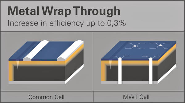
Metal Wrap Through
Using laser structuring machines, it is possible to implement several different performance enhancing technologies. A common method for increasing cell efficiency is „Metal Wrap Through” (MWT). This method essentially reduces metallization on the front-side of the cell, which in turn reduces the shadowing effect of the received sunlight. The reduction in shading is achieved by moving some of the front side contacts to the back of the cell, which consequently reduces the front-side metallized area by almost 50 % and increases the efficiency of the cell by up to 0.3 %. Three specific process steps in the manufacturing process of a MWT cell differentiate it from the standard cell. Firstly, a laser scribes several holes into the solar cell. These holes are later filled with solar paste, thus creating through-hole vias, i.e. an electrical connection from the front to the back of the cell. Finally, a slight modification of the backside contacts is made. For the production of MWT-cells, there is offered a high performance, highly accurate and cost-effective laser system. To make the holes, the company provides modular based laser systems in an island configuration using the existing platform of the SEI01 Laser System. The modular design plays a particularly important role in the design process at Asys, which allows easy integration of loaders and unloaders into the system.
Since the front-side contact surfaces are significantly reduced, this gives MWT cells a very particular appearance. The cells look rather darker and more homogeneous than normal cells which make them very popular with the end-users. The advantages of MWT also become particularly evident when any modifications to the cells are required. The through-contacting means that the connectors must no longer go from the front to the backside of the next cell, which not only allows the cells to be more tightly packed into the modules but also increases the degree of automation used in module manufacture. Consequently, larger connectors are used on the backside of the cell which also provides lower power dissipation by lower conduction. The high cost saving potential, together with the increase in efficiency associated with reduced shadowing, easily justifies the additional process steps in the production of MWT cells. The rise in efficiency and the reduction in the module construction costs make the Metal Wrap Through technology a particularly cost-effective solution.
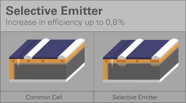
Selective Emitter
A high doping concentration on the emitter side of industrially manufactured crystalline silicon solar cells is on one hand a positive feature which allows lower conduction loss, but also one which results in higher losses when converting sunlight to electrical current since a considerable part of the absorbed light is lost as heat due to recombination effects. The selective emitter technology (SE) works with a selective diffusion structure on the emitter side of the cell. To reduce the contact resistance, various processes are utilized to produce an increased concentration of dopant atoms underneath the metalizing contacts. At the same time, a reduced concentration of dopant atoms is created between the metallization contacts resulting in a more effective cell surface area that converts more sunlight into electric current. Increases in efficiency of up to 0.8% are possible with the use of SE technology. The company also offers laser processing modules for cost effective manufacture of selective emitter cells, additionally highly repeatable screen printers are ideally suited for accurate placement of metallization lines on top of the selectively doped regions.
Unsere Webinar-Empfehlung
Applikationen aus dem Bereich der Leistungselektronik gewinnen immer mehr an Bedeutung. Die Inspektion dieser Applikation lässt sich mit der bewährten Standardtechnologie der 3D-Messtechnik bewerkstelligen.
Teilen:


