Using DirEKt Imaging as an enabling technology, interconnects with pitches as fine as 0.25mm can now be created in production wafer bumping applications. Cycle time is independent of I/O count, supporting high-volume production. The potential advantages of using stencils in wafer bumping have been well-recognized. The combination of DEK’s patented ProFlow technology with precision stencils and custom-designed wafer handling equipment allows significant savings to be realized in capital investment, process complexity and overall process footprint. In addition, it enables the achievement of higher levels of throughput. The system consists of a fully enclosed transfer head containing a paste cassette, conditioning chamber and paste retention system. Material within the cassette is not exposed to the environment until it is propelled through the stencil. As the print head traverses the surface of the stencil, the apertures are filled uniformly and rapidly, without residual paste being left on the stencil surface, for dramatic reductions in paste wastage. The technology is fully cleanroom compatible.
EPP 178
Unsere Webinar-Empfehlung
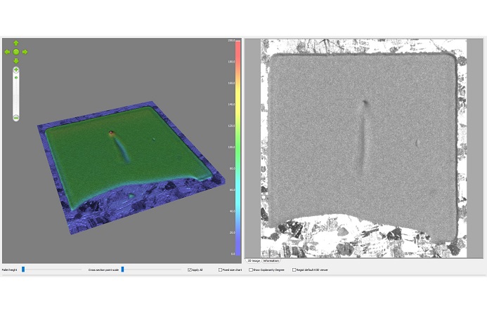
Applikationen aus dem Bereich der Leistungselektronik gewinnen immer mehr an Bedeutung. Die Inspektion dieser Applikation lässt sich mit der bewährten Standardtechnologie der 3D-Messtechnik bewerkstelligen.
Teilen:


